You are currently viewing SemiWiki as a guest which gives you limited access to the site. To view blog comments and experience other SemiWiki features you must be a registered member. Registration is fast, simple, and absolutely free so please,
join our community today!
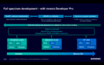
At the heart of the shift-left strategy is the goal of moving traditionally late-stage tasks—such as software development, validation, and optimization—earlier in the design process. This proactive approach allows teams to identify and resolve issues before they escalate, reducing costly rework and shortening the overall… Read More
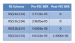
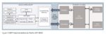
As digital transmission speeds increase, designers use various techniques to improve the signal-to-noise ratio at the receiver output. One such technique is the Decision Feedback Equalizer (DFE) scheme, commonly used in high-speed Serializer-Deserializer (SerDes) circuits to mitigate the effects of channel noise and … Read More
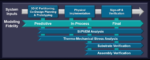
An earlier blog started with the topic of delivering 3D IC innovations faster. The blog covered the following foundational enablers for successful heterogeneous 3D IC implementation.
- System Co-Optimization (STCO) approach
- Transition from design-based to systems-based optimization
- Expanding the supply chain and tool
…
Read More
3D IC technology development started many years ago well before the slowing down of Moore’s law benefits became a topic of discussion. The technology was originally leveraged for stacking functional blocks with high-bandwidth buses between them. Memory manufacturers and other IDMs were the ones to typically leverage this … Read More
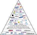
The last year has seen a ton written about the semiconductor industry: chip shortages, the CHIPS Act, our dependence on Taiwan and TSMC, China, etc.
But despite all this talk about chips and semiconductors, few understand how the industry is structured. I’ve found the best way to understand something complicated is to diagram… Read More
A decade ago, many of us heard commentaries on how entrepreneurs were turned down by venture capitalists for not including a cloud strategy in their business plan, no matter what the core business was. Humorous punchlines such as, “It’s cloudy without any clouds” and “Add some cloud to your strategy and your future will be bright… Read More
Silicon photonics is getting a lot of interest because it can be used in many applications to improve bandwidth, reduce power and provide novel new functionality. It is especially interesting because it offers an ability to combine electronics and optical elements into the same die. Though it is fabricated with familiar silicon… Read More
UPF was created to go beyond what HDL can do for managing on-chip power. HDLs are agnostic when it comes to dealing with supply & ground connections, power domains, level shifters, retention and other power management related elements of SoCs. UPF fills the breach allowing designers to specify in detail what parts of the design… Read More
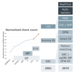
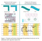
All semiconductor design work today rests on the three-legged stool of Foundries, EDA Tools and Designers. Close collaboration between the three make possible the successful completion of ever more complex designs, especially those at advanced nodes. Perhaps one of the most critical intersections of all three is during physical… Read More
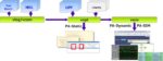
PCI Express (PCIe) has become an important communication element in a wide range of systems. It is used to connect networking, storage, FPGA and GPGPU boards to servers and desktop systems. It has progressed a long way from its initial parallel bus format. Its evolution to a serial point to point configuration has been accompanied… Read More