The last year has seen a ton written about the semiconductor industry: chip shortages, the CHIPS Act, our dependence on Taiwan and TSMC, China, etc.
But despite all this talk about chips and semiconductors, few understand how the industry is structured. I’ve found the best way to understand something complicated is to diagram it out, step by step. So here’s a quick pictorial tutorial on how the industry works.
The Semiconductor Ecosystem
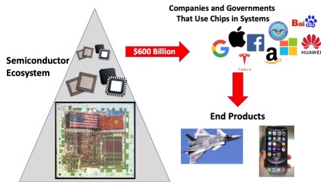
We’re seeing the digital transformation of everything. Semiconductors – chips that process digital information — are in almost everything: computers, cars, home appliances, medical equipment, etc. Semiconductor companies will sell $600 billion worth of chips this year.
Looking at the figure below, the industry seems pretty simple. Companies in the semiconductor ecosystem make chips (the triangle on the left) and sell them to companies and government agencies (on the right). Those companies and government agencies then design the chips into systems and devices (e.g. iPhones, PCs, airplanes, cloud computing, etc.), and sell them to consumers, businesses, and governments. The revenue of products that contain chips is worth tens of trillions of dollars.
Yet, given how large it is, the industry remains a mystery to most. If you do think of the semiconductor industry at all, you may picture workers in bunny suits in a fab clean room (the chip factory) holding a 12” wafer. Yet it is a business that manipulates materials an atom at a time and its factories cost 10s of billions of dollars to build. (By the way, that wafer has two trillion transistors on it.)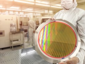
If you were able to look inside the simple triangle representing the semiconductor industry, instead of a single company making chips, you would find an industry with hundreds of companies, all dependent on each other. Taken as a whole it’s pretty overwhelming, so let’s describe one part of the ecosystem at a time. (Warning – this is a simplified view of a very complex industry.)
Semiconductor Industry Segments
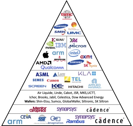
The semiconductor industry has seven different types of companies. Each of these distinct industry segments feeds its resources up the value chain to the next until finally a chip factory (a “Fab”) has all the designs, equipment, and materials necessary to manufacture a chip. Taken from the bottom up these semiconductor industry segments are:
- Chip Intellectual Property (IP) Cores
- Electronic Design Automation (EDA) Tools
- Specialized Materials
- Wafer Fab Equipment (WFE)
- “Fabless” Chip Companies
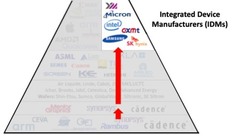
- Integrated Device Manufacturers (IDMs)
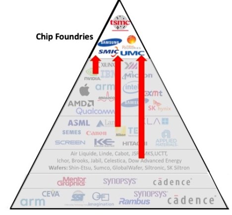
- Chip Foundries
The following sections below provide more detail about each of these seven semiconductor industry segments.
Chip Intellectual Property (IP) Cores
- The design of a chip may be owned by a single company, or…
- Some companies license their chip designs – as software building blocks, called IP Cores – for wide use
- There are over 150 companies that sell chip IP Cores
- For example, Apple licenses IP Cores from ARM as a building block of their microprocessors in their iPhones and Computers
Electronic Design Automation (EDA) Tools
- Engineers design chips (adding their own designs on top of any IP cores they’ve bought) using specialized Electronic Design Automation (EDA) software
- The industry is dominated by three U.S. vendors – Cadence, Mentor (now part of Siemens) and Synopsys
- It takes a large engineering team using these EDA tools 2-3 years to design a complex logic chip like a microprocessor used inside a phone, computer or server. (See the figure of the design process below.)
- Today, as logic chips continue to become more complex, all Electronic Design Automation companies are beginning to insert Artificial Intelligence aids to automate and speed up the process
Specialized Materials and Chemicals
So far our chip is still in software. But to turn it into something tangible we’re going to have to physically produce it in a chip factory called a “fab.” The factories that make chips need to buy specialized materials and chemicals:
- Silicon wafers – and to make those they need crystal growing furnaces
- Over 100 Gases are used – bulk gases (oxygen, nitrogen, carbon dioxide, hydrogen, argon, helium), and other exotic/toxic gases (fluorine, nitrogen trifluoride, arsine, phosphine, boron trifluoride, diborane, silane, and the list goes on…)
- Fluids (photoresists, top coats, CMP slurries)
- Photomasks
- Wafer handling equipment, dicing
- RF Generators
Wafer Fab Equipment (WFE) Make the Chips
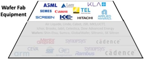
- These machines physically manufacture the chips
- Five companies dominate the industry – Applied Materials, KLA, LAM, Tokyo Electron and ASML
- These are some of the most complicated (and expensive) machines on Earth. They take a slice of an ingot of silicon and manipulate its atoms on and below its surface
- We’ll explain how these machines are used a bit later on
“Fabless” Chip Companies
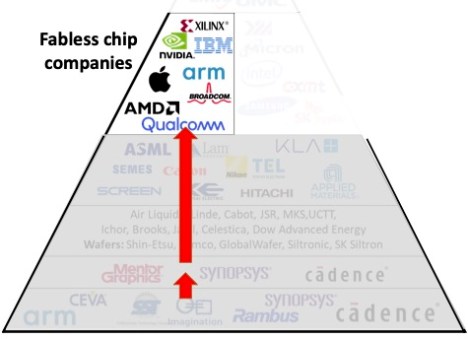
- Systems companies (Apple, Qualcomm, Nvidia, Amazon, Facebook, etc.) that previously used off-the-shelf chips now design their own chips.
- They create chip designs (using IP Cores and their own designs) and send the designs to “foundries” that have “fabs” that manufacture them
- They may use the chips exclusively in their own devices e.g. Apple, Google, Amazon ….
- Or they may sell the chips to everyone e.g. AMD, Nvidia, Qualcomm, Broadcom…
- They do not own Wafer Fab Equipment or use specialized materials or chemicals
- They do use Chip IP and Electronic Design Software to design the chips
Integrated Device Manufacturers (IDMs)
- Integrated Device Manufacturers (IDMs) design, manufacture (in their own fabs), and sell their own chips
- They have their own “fabs” but may also use foundries
- They use Chip IP and Electronic Design Software to design their chips
- They buy Wafer Fab Equipment and use specialized materials and chemicals
- The average cost of taping out a new leading-edge chip (3nm) is now $500 million
Chip Foundries
- Foundries make chips for others in their “fabs”
- They buy and integrate equipment from a variety of manufacturers
- Wafer Fab Equipment and specialized materials and chemicals
- They design unique processes using this equipment to make the chips
- But they don’t design chips
- TSMC in Taiwan is the leader in logic, Samsung is second
- Other fabs specialize in making chips for analog, power, rf, displays, secure military, etc.
- It costs $20 billon to build a new generation chip (3nm) fabrication plant
Fabs
- Fabs are short for fabrication plants – the factory that makes chips
- Integrated Device Manufacturers (IDMs) and Foundries both have fabs. The only difference is whether they make chips for others to use or sell or make them for themselves to sell.
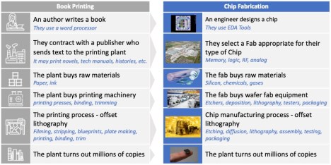
- Think of a Fab as analogous to a book printing plant (see figure below)
- Just as an author writes a book using a word processor, an engineer designs a chip using electronic design automation tools
- An author contracts with a publisher who specializes in their genre and then sends the text to a printing plant. An engineer selects a fab appropriate for their type of chip (memory, logic, RF, analog)
- The printing plant buys paper and ink. A fab buys raw materials; silicon, chemicals, gases
- The printing plant buys printing machinery, presses, binders, trimmers. The fab buys wafer fab equipment, etchers, deposition, lithography, testers, packaging
- The printing process for a book uses offset lithography, filming, stripping, blueprints, plate making, binding and trimming. Chips are manufactured in a complicated process manipulating atoms using etchers, deposition, lithography. Think of it as an atomic level offset printing. The wafers are then cut up and the chips are packaged
- The plant turns out millions of copies of the same book. The plant turns out millions of copies of the same chip
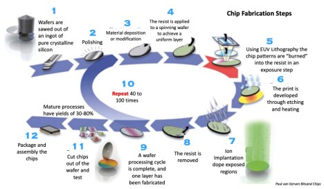
 While this sounds simple, it’s not. Chips are probably the most complicated products ever manufactured. The diagram below is a simplified version of the 1000+ steps it takes to make a chip.
Fab Issues
- As chips have become denser (with trillions of transistors on a single wafer) the cost of building fabs have skyrocketed – now >$10 billion for one chip factory
- One reason is that the cost of the equipment needed to make the chips has skyrocketed
- Just one advanced lithography machine from ASML, a Dutch company, costs $150 million
- There are ~500+ machines in a fab (not all as expensive as ASML)
- The fab building is incredibly complex. The clean room where the chips are made is just the tip of the iceberg of a complex set of plumbing feeding gases, power, liquids all at the right time and temperature into the wafer fab equipment
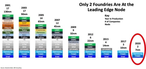
- The multi-billion-dollar cost of staying at the leading edge has meant most companies have dropped out. In 2001 there were 17 companies making the most advanced chips. Today there are only two – Samsung in Korea and TSMC in Taiwan.
- Given that China believes Taiwan is a province of China this could be problematic for the West.
 What’s Next – Technology
It’s getting much harder to build chips that are denser, faster, and use less power, so what’s next?
- Instead of making a single processor do all the work, logic chip designers have put multiple specialized processors inside of a chip
- Memory chips are now made denser by stacking them 100+ layers high
- As chips are getting more complex to design, which means larger design teams, and longer time to market, Electronic Design Automation companies are embedding artificial intelligence to automate parts of the design process
- Wafer equipment manufacturers are designing new equipment to help fabs make chips with lower power, better performance, optimum area-to-cost, and faster time to market
What’s Next – Business
The business model of Integrated Device Manufacturers (IDMs) like Intel is rapidly changing. In the past there was a huge competitive advantage in being vertically integrated i.e. having your own design tools and fabs. Today, it’s a disadvantage.
- Foundries have economies of scale and standardization. Rather than having to invent it all themselves, they can utilize the entire stack of innovation in the ecosystem. And just focus on manufacturing
- AMD has proven that it’s possible to shift from an IDM to a fabless foundry model. Intel is trying. They are going to use TSMC as a foundry for their own chips as well as set up their own foundry
What’s Next – Geopolitics
Controlling advanced chip manufacturing in the 21st century may well prove to be like controlling the oil supply in the 20th. The country that controls this manufacturing can throttle the military and economic power of others.
- Ensuring a steady supply of chips has become a national priority. (China’s largest import by $’s are semiconductors – larger than oil)
- Today, both the U.S. and China are rapidly trying to decouple their semiconductor ecosystems from each other; China is pouring $100+ billion of government incentives in building Chinese fabs, while simultaneously trying to create indigenous supplies of wafer fab equipment and electronic design automation software
- Over the last few decades the U.S. moved most of its fabs to Asia. Today we are incentivizing bringing fabs and chip production back to the U.S.
An industry that previously was only of interest to technologists is now one of the largest pieces in great power competition.
Also read:
TSMC Earnings – The Handoff from Mobile to HPC
Intel Discusses Scaling Innovations at IEDM
Share this post via:






Is Intel About to Take Flight?