3D IC technology development started many years ago well before the slowing down of Moore’s law benefits became a topic of discussion. The technology was originally leveraged for stacking functional blocks with high-bandwidth buses between them. Memory manufacturers and other IDMs were the ones to typically leverage this technology during its early days. As the technology itself does not limit the use to only such purposes, there has always been a broader appeal and potential for this technology.
Over the years, 3D IC technology has progressed from its novelty stage to becoming an established mainstream manufacturing technology. And the EDA industry has introduced many tools and technology to help design products that take the 3D IC path. Over the recent past, complex SoC implementations started leveraging 3D IC technology to balance performance/cost goals.
The slowing of Moore’s law has become a major driver to the chiplets way of implementing SoCs. Chiplets are small ICs specifically designed and optimized for operation within a package in conjunction with other chiplets and full-sized ICs. More companies are turning to 3D stacking of ICs and chiplets implemented in different process nodes optimal for the respective chiplet’s function. Designers can also combine 3D memory stacks, such as high bandwidth memory, on a silicon interposer within the same package. The 3D IC implementation will be a major beneficiary of the chiplets adoption wave.
When a new capability is ready for mainstream, its mass adoption success depends on how easily, quickly, effectively and efficiently a solution can be delivered. While the 3D IC manufacturing technology may have become mainstream, there are some foundational enablers for a successful heterogeneous 3D IC implementation. Siemens EDA recently published an eBook on this topic, authored by Keith Felton.
This post will highlight some salient points from the eBook. A follow up post will cover methodology and workflows recommendations for achieving optimal results when implementing 3D IC designs.
Foundational Enablers For Successful Heterogeneous 3D IC Implementation
Any good design methodology always includes look-aheads for downstream effects in order to consider and address them early in the design process. While this is important for monolithic designs, it becomes paramount when designing 3D ICs.
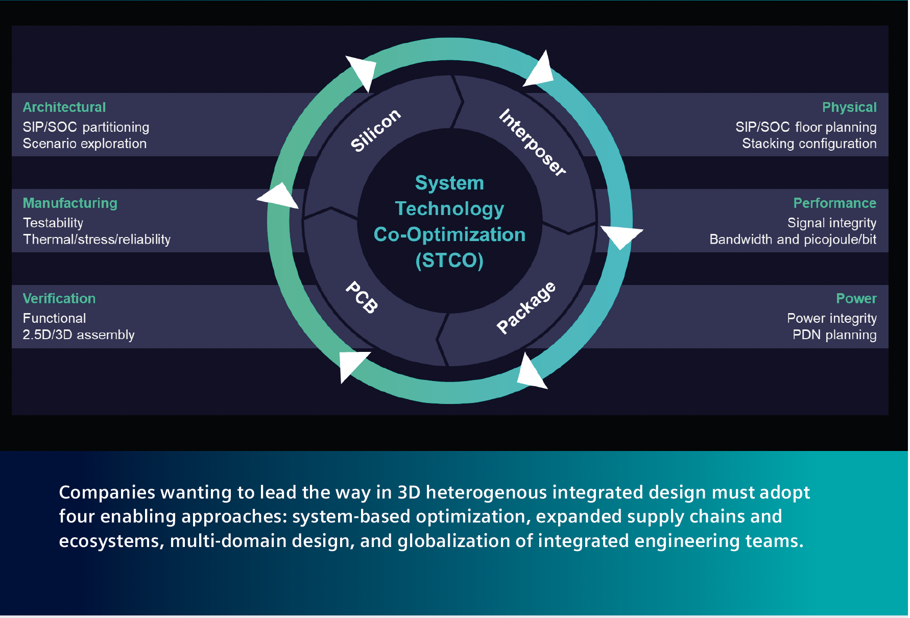
System Co-Optimization (STCO) approach
This approach involves starting at the architectural level to partition the system into various chiplets and packaged die based on functional requirements and form factor constraints. After this step, RTL or functional models are generated. This is followed by physical floor planning and validation all the way to detailed layout supported with in-process performance modeling.
STCO elements already exist in a number of Siemens EDA tools, allowing engineers to evaluate design decisions in the context of predictive downstream effects of routability, power, thermal and manufacturability. Predictive modeling is a fundamental component of the STCO methodology that leverages Siemens EDA modeling tools during physical planning to gain early insight into downstream performance.

Transition from design-based to systems-based optimization
A 3D IC design requires consistent system representation throughout the design and integration process with visibility and interoperability of all cross-domain content. This calls for tools and methodology capable of a full system perspective from early planning through implementation to design signoff and manufacturing handoff.
Expanding the supply chain and tool ecosystem
3D IC design efforts demand a higher level of tool interoperability and openness than the industry is used to. Sharing and updating design content in a multi-vendor and/or multi-tool environment must be supported. This places a greater demand on assembly level verification throughout the design process to ensure the different pieces of the system work together as expected.
Balancing design resources across multiple domains
STCO facilitates exploration of the 3D IC solution space for striking the ideal balance of resources across all domains and deriving the optimal product configuration. An early perspective enables better engineering decisions on resource allocation, resulting in higher performing, more cost effective products.
Tighter integration of the various teams
A new design flow is required to support the design, validation, and integration of multiple ASICs, chiplets, memory, and interposers within a 3D IC design. The silicon, packaging and PCB teams are more likely to be global, requiring even tighter integration with the system, RTL and ASIC design processes.
For more details on Siemens EDA 3D IC innovations, you can download the eBook published by Siemens EDA.
While the Siemens heterogeneous 3D IC solution is packed with powerful capabilities, fully benefitting from these capabilities depends on the implementation methodology put to use. Designing 3D IC products that deliver differentiation, profitability and time to market advantages will be the subject of a follow-on blog.
Also Read:
Coverage Analysis in Questa Visualizer
EDA in the Cloud with Siemens EDA at #59DAC
Calibre, Google and AMD Talk about Surge Compute at #59DAC
Share this post via:


Comments
There are no comments yet.
You must register or log in to view/post comments.