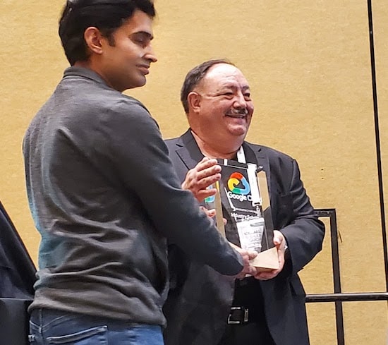

In 2022 using the cloud for EDA tasks is a popular topic, and at DAC this year I could see a bigger presence from the cloud hardware vendors in the exhibit area, along with a growing stampede of EDA companies. Tuesday at DAC there was a luncheon with experts from Siemens EDA, Google and AMD talking about surge compute. I already knew Michael White of Siemens EDA who was moderator, while Peeyush Tugnawat of Google, and Philip Steinke of AMD were new faces to me. There was an award presented from Google Cloud for Industry Solutions Partner of the Year 2020, and Michael Buehler-Garcia graciously received it for Siemens EDA.

Cloud for Surge Compute, Why Now?
The relentless pursuit of Moore’s Law brings us ever-small nodes, which then dramatically increase the computation requirements for EDA tools, like: physical verification, circuit simulation, DFM, DFT, functional verification, and more. The CPU cycles with most on-premise design teams isn’t enough to meet timelines, so that’s when cloud capacity comes to the rescue.

Google’s View
Peeyush opened by sharing that Google has some $257B in revenue, from 9 services, attracting 1B+ active users, and that their Cloud Business revenue is $20B, so yes, cloud is a priority. Silicon design has huge CPU needs across compute, storage and network. He showed a cool diagram of the chip design process, and denoted which segments were compute intensive or data intensive.

Google Cloud offers three VMs for general purpose, and three VMs for workload-optimized, so there’s a lot of flexibility for EDA users to choose the best VM for the task at hand. Scaling happens by deploying up to 1,000 instances with a single call. Google Cloud also partners with the most popular file systems: NetApp, Dell Powerscale, DDN EXAScaler, IBM Spectrum Scale, Intel DAOS. The internal Google Cloud network is global, and secure, built without public hubs to increase security.
AMD’s View
Google Cloud has VMs that are powered by AMD EPYC processors, that enable complex EDA workloads to run faster. Phil mentioned that having Google Cloud as a partner has enabled their HW teams to tackle the biggest processor designs while meeting aggressive TTM goals. The specific instances with AMD EPYC processors were N2D, C2D and T2D. The SoC design example was the AMD Raden MI50 GPU, having an impressive 13.2B transistors, a high-performance compute engine, scalable interconnect, end-to-end ECC enablement, fabricated at TSMC on the N7 node.

Siemen’s EDA View
Michael White presented how Calibre PERC was run on a large design in Google Cloud with AMD servers, comparing the performance of N2D and C2D, where 16 to 816 CPUs were used. With just 16 CPUs the run time was about 5 days on the 2nd generation N2D, while using 816 CPUs the run time shrunk to just 8 hours on the 3rd generation C2D. Using more CPUs enables a design team to get 2 iterations per day, so that’s a big time savings using surge compute.

The memory footprint for Calibre PERC was smaller than competitors tools, and pretty much flat with more cores added, making the approach quite efficient. Even full-chip P2P checks on the I/O ring could now be run overnight using surge compute on the MI50 GPU design. Data was shared on how Calibre nmDRC was run on the MI50 GPU design with up to 1,500 CPUs, enabling 6 iterations per day.

Summary
Yes, Moore’s Law is still alive, and these leading-edge process nodes are dramatically increasing CPU requirements for EDA tools, calling in to question the sole reliance of on-premise computing. Using the power of the cloud really is meeting the compute challenges, and the collaboration between AMD, Google Cloud and Siemens EDA has worked out quite well. EDA jobs that used to take multiple days, can now be iterated several times per day by using the cloud.
There is some circular reinforcement going on here, because AMD designers are using AMD hardware to design the next generation of AMD hardware, thanks to the infrastructure of Google Cloud combined with the software from EDA vendors like Siemens EDA.
Related Blogs
- DAC 2021 – Siemens EDA talks about using the Cloud
- Library Characterization: A Siemens Cloud Solution using AWS
- EDA in the Cloud – Now More Than Ever
- Calibre Commences Cloud Computing
- Intel Foundry Services Puts PDKs in the Cloud
- Slash Tapeout Times with Calibre in the Cloud


Comments
There are no comments yet.
You must register or log in to view/post comments.