
At the recent User2user conference, Amit Kumar, Principal Hardware Engineer, Microsoft, shared the company’s experience from building a 3DIC SoC and highlighted Siemens EDA tools that were used. The following is a synthesis of core aspects of that talk.
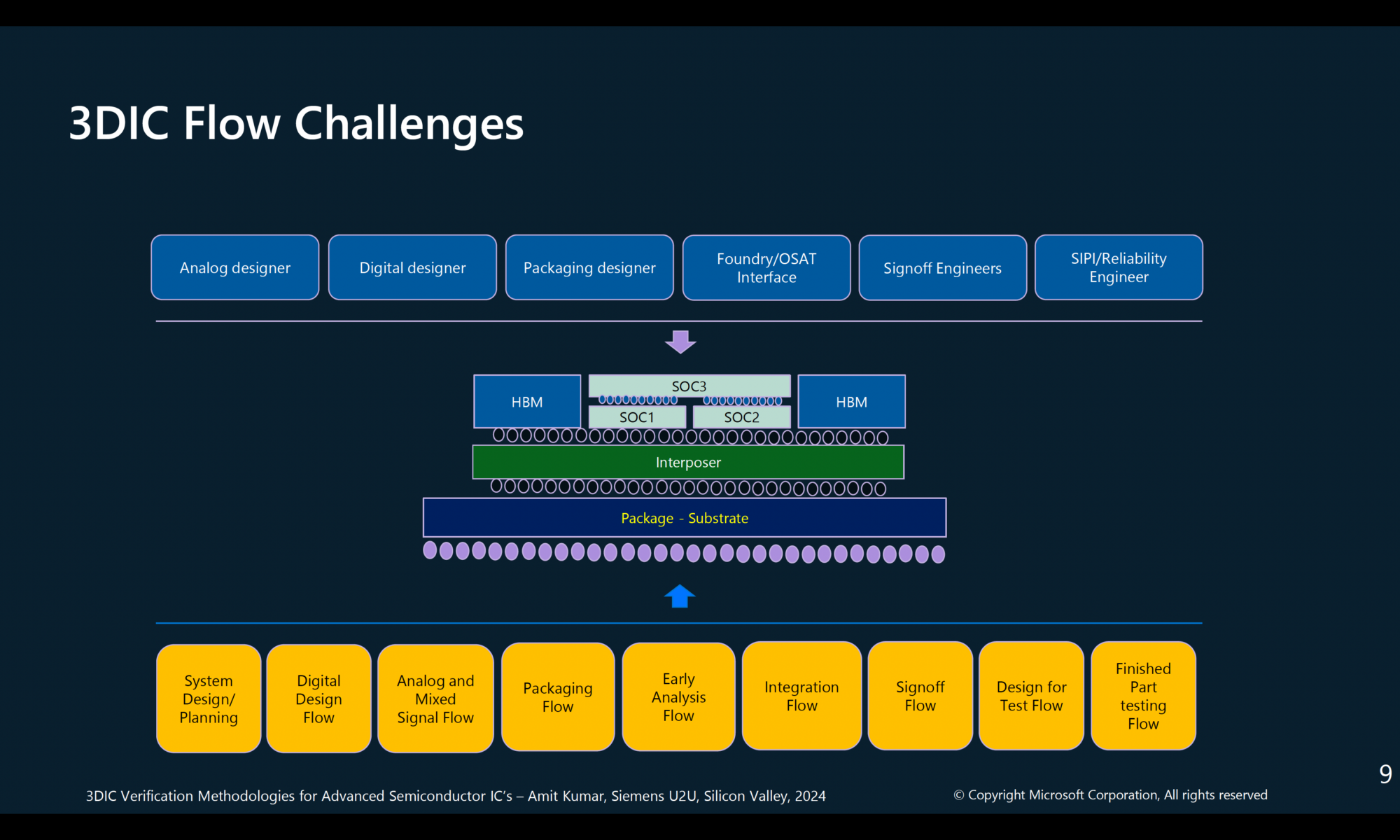
3DIC Challenges
Despite the numerous advantages of 3DIC technology, its adoption is accompanied by several challenges. These include higher overall system costs, lower yield for the whole system, increased power density and thermal management difficulties, design complexity, Through-Silicon Vias (TSV) overhead, timing variation uncertainties, the need for new testing and verification methods, hierarchical and modular design requirements, and a lack of standards. Addressing these challenges requires collaborative efforts from industry stakeholders to develop innovative solutions, adopt best practices, and establish industry standards, ultimately unlocking the full potential of 3DIC technology for next-generation electronic systems.
3DIC Flow & Data Management Challenges
3DICs introduce a host of challenges, particularly in design flow and data management. Integrating heterogeneous technologies and managing complex interconnections across multiple layers demand robust data management solutions and comprehensive verification methodologies. Ensuring design integrity and reliability while navigating the intricate 3DIC landscape requires meticulous attention to detail and innovative approaches to data handling.


TSMC 3DBlox Open Standard
The 3DBlox technology is an open-source standard and promotes interoperability and collaboration across the semiconductor industry. TSMC’s 3DBlox 1.0 laid the foundation for 3D integration, enabling designers to stack logic and memory dies with TSVs for improved performance and power efficiency. Building upon this foundation, TSMC unveiled 3DBlox 2.0, further enhancing the scalability and flexibility of 3DIC designs with advanced packaging options and improved interconnect technologies. This includes ability to stack chips manufactured on different process nodes, enabling heterogeneous integration and maximizing design flexibility.
Design, Physical Verification, Reliability Analysis for 3DIC
Designing a 3DIC involves a multifaceted process encompassing design, physical verification, and reliability analysis. Designers must meticulously craft layouts that optimize performance, minimize power consumption, and ensure compatibility with heterogeneous technologies. Physical verification and reliability analysis are equally critical, encompassing checks for Design Rule Violations (DRV), Layout versus Schematic (LVS) verification, and reliability assessments such as thermal analysis and electromigration checks.
3DIC Verification Flow
Microbump libraries and Power Delivery Network (PDN) delivery are crucial for efficient signal routing and power distribution in 3DIC design. Microbump libraries offer optimized configurations for inter-die connections, while PDN delivery ensures robust power distribution for high-performance 3DICs. Verification at the die, package, and interposer levels is vital for seamless integration. Die-level verification ensures compliance and reliability, while package and interposer verification validate system integrity, covering signal, thermal, and mechanical aspects. The verification flow includes standalone verification of package-interposer layers, integrated verification, and staged approaches for early issue identification and resolution, ensuring the integrity and reliability of 3DIC designs.
Physical Verification Using Siemens EDA Tools
Verification using Siemens XSI (Xpedition Substrate Integrator) and Calibre 3DSTACK together offer a comprehensive solution for validating the integrity, functionality, and manufacturability of 3DIC designs. These tools leverage heterogeneous data sources, including ODB++, GDS, OASIS, LEF/DEF, and Verilog formats, to build a full system model encompassing all components and layers of the 3DIC design. They generate system-level netlists suitable for Layout vs. Schematic (LVS) and Static Timing Analysis (STA), enabling comprehensive verification of connectivity and timing characteristics. With support for detailed connectivity visualization, device transformation, and creation of interconnected devices, XSI and Calibre 3DSTACK facilitate the seamless integration and validation of 3DIC designs, ensuring successful development and deployment of high-performance and reliable solutions.
Calibre 3DSTACK
Calibre 3DSTACK is essential for verifying the integrity of stacked dies in 3DIC design. It utilizes data from XSI and specific physical details to configure checks for design rules and connectivity. The tool offers a range of checks, focusing on port and text attributes, which users can customize based on their requirements. By detecting issues like floating texts and verifying port connectivity, Calibre 3DSTACK ensures the reliability and manufacturability of 3DIC designs. It integrates seamlessly with XSI, enabling accurate verification and analysis for high-performance 3DIC solutions.
XSI Utilities and Automation
XSI simplifies 3DIC design projects with its utilities and automation features. It enables project database creation, data extraction, and setup propagation for efficient project management. The tool’s bump file splitting utility categorizes bump data, while automatic text identification and alignment streamline text manipulation. Property propagation ensures consistency, and runset creation automates connectivity checks, enhancing verification efficiency. These capabilities enhance productivity and accuracy in 3DIC design workflows, leading to optimal results in design and verification.
Optical Shrink and Thermal Expansion Handling
Optical shrink and thermal expansion pose unique challenges in 3DIC design, necessitating specialized methodologies and tools for accurate modeling. Optical shrink refers to feature distortion during lithography, while thermal expansion affects stacked die stability. XSI and Calibre 3DSTACK support die shrinking and optical shrink, ensuring functionality while reducing feature sizes. Verification tools address die shrinking mismatches, ensuring proper alignment and connectivity between stacked dies. Thermal expansion coefficients are considered to predict and mitigate package expansion effects. Thermal mechanical analysis evaluates thermal expansion impact on 3DIC stack integrity.
Summary
The journey towards realizing the full potential of 3DIC technology is marked by challenges and opportunities. From data management and design flow challenges to physical verification and reliability analysis, each aspect of 3DIC design demands meticulous attention and innovative solutions. By leveraging cutting-edge tools and methodologies, designers can navigate the complexities of 3DIC design and unlock new possibilities for high-performance and compact electronic systems. Siemens EDA is working closely across the ecosystem to deliver cutting edge tools and methodologies that support multi-vendor flow.
Also Read:
Rigid-flex PCB Design Challenges
Will my High-Speed Serial Link Work?
Enabling Imagination: Siemens’ Integrated Approach to System Design
Share this post via:


Comments
There are no comments yet.
You must register or log in to view/post comments.