
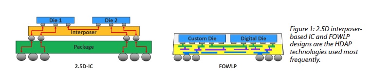
Innovations in packaging have played an important role in improving system performance and area utilization. Advances like 2.5D interposers and fan-out wafer-level packaging (FOWLP) have allowed mixed dies to be used in a single package and have dramatically reduced the number of connections that need to go all the way to the PCB level. Mixed dies allows for mixing process nodes and combining different types of chip, or chiplets, in a single package. Also every time a net needs to travel to a PCB, there are issues with delay, coupling and transmission line effects, among other things. Yet despite their advantages these high density advanced packaging (HDAP) introduce more complexity into package verification. By moving what used to be on-chip or on-board signals into the package, complexity goes up greatly. At the same time the mature approaches for PCB or IC LVS and LVL cannot easily be applied to this problem.
Mentor has recently published a technical paper entitled “A deep dive into HDAP LVS/LVL verification” written by Tarek Ramadan, that looks closely at the verification challenges which arrive when HDAP is used. There are a host of issues that stem from how new much of the technology is.
The ownership of design and verification for HDAP can vary from organization to organization and from chip to chip. Often, interposer designs are considered more chip centric and the responsibility can fall to the silicon teams. For FOWLP opposite can be the case and packaging teams may be tasked with verification.
Because of the interdependence between the IC’s and the package interconnect, package verification might have to wait for die information to stabilize and be delivered, which can delay the entire design. The paper describes the methods that can be used to permit parallel work to avoid schedule impacts.
Another complicating factor is that unlike IC processes, the ‘stack up’ for a package may vary from design to design due to the specifics of the chips and how they can be most efficiently combined. This prevents the use of off the shelf PDK-like information for layer and pin definitions. The tools used in these flows must be flexible and have the ability to adapt to design specific configurations easily.
To help readers understand the possibilities, the Mentor paper goes through several cases that illustrate how LVS and LVL verification can be completed in various scenarios. The first case deals with what happens when there is no explicit schematic for the interconnect in the package. Of course, with simpler technologies spreadsheets sufficed for determining correct package connections. The efficacy of spreadsheets goes down with the increased complexity of HDAP. The Mentor paper describes how labels on the geometry can be used to overcome these issues and help detect shorts and opens in these designs.
The other limitation that is encountered when trying to use chip level LVS and LVL tools is that there are no devices per se in the package netlist. The paper talks about how assembly level tools can work around this issue by creating placeholders for the pins in the package. There are a number of variations where the data needed is not directly available and the flows must accommodate this.
Based on their understanding of the issues enumerated in the paper, Mentor offers several tools that facilitate LVL and LVS verification of HDAP designs. Their Xpedition™ Substrate Integrator (xSI) tool performs HDAP system-level connectivity management and planning. Calibre 3DSTACK HDAP, used in conjunction with xSI, can run all the flows outlined in the paper, providing solutions for most cases. The paper makes good reading and can be downloaded from the Mentor website.
Share this post via:


Comments
There are no comments yet.
You must register or log in to view/post comments.