You are currently viewing SemiWiki as a guest which gives you limited access to the site. To view blog comments and experience other SemiWiki features you must be a registered member. Registration is fast, simple, and absolutely free so please,
join our community today!
SkyWater Technology, a U.S. based pure-play semiconductor foundry, has made significant strides in 2025 reinforcing its position as a leader in domestic semiconductor manufacturing. Headquartered in Bloomington, Minnesota, SkyWater specializes in advanced innovation engineering and high volume manufacturing of differentiated… Read More
Innovations in packaging have played an important role in improving system performance and area utilization. Advances like 2.5D interposers and fan-out wafer-level packaging (FOWLP) have allowed mixed dies to be used in a single package and have dramatically reduced the number of connections that need to go all the way to the… Read More
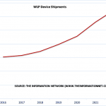
Advanced IC packaging, such as fan-out WLP (Wafer Level Packaging) and 2.5D TSV (Through Silicon Via) will drive the packaging equipment market, particularly lithography. This will help specific equipment manufacturers in 2019, since the WFE (Wafer Front End) market will drop 17%. But the Back-End lithography market, led … Read More
DesignCon is coming up, kicking off the first of many industry conferences for the year. It’s at the Santa Clara Convention Center which is the best venue in Northern California. Not only is this a semiconductor crowd, it’s also a systems crowd covering chips, boards, and systems. More than 175 companies participate with an expected… Read More
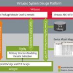
With each new silicon process node, the complexity of SoC design rules and physical verification requirements increases significantly. The foundry and an EDA vendor collaborate to provide a “reference flow” – a set of EDA tools and process design kit (PDK) data that have been qualified for the new node. SoC design methodology … Read More
This week, we are continuing our discussion of various topics that Semitracks addresses in their training activities. One area that they focus on quite a bit is Semiconductor Reliability and Product Qualification.
One of the key activities that a Product Engineer will coordinate is the qualification of new products before they… Read More
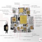
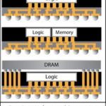
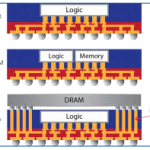
Regular Semiwiki readers are aware of the rapid emergence of various (multi-die) advanced package technologies, such as: FOWLP (e.g., Amkor’s SWIFT, TSMC’s InFO); 2D die placement on a rigid substrate (e.g., TSMC’s CoWoS); and, 2.5D “stacked die” with vertical vias (e.g., any of the High Bandwidth Memory,… Read More
There is an emerging set of advanced packaging technologies that enables unique product designs, with the capability to integrate multiple die, from potentially heterogeneous technologies. These “system-in-package” (SiP) offerings provide architects with the opportunity to optimize product performance, power, cost,… Read More
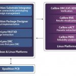
I caught up with John Ferguson of Mentor Graphics this week to learn more about a recent announcement that TSMC has extended its collaboration with Mentor in the area of Fan-Out Wafer Level Processing (FOWLP).
In March of last year Mentor and TSMC announced that they were collaborating on a design and verification flow for TSMC’s… Read More
In constant pursuit of improved performance, power and cost, chip and system designers always want to integrate more functions together because this minimizes inter-device loads (affecting performance and power) and bill of materials on the board (affecting cost). However it generally isn’t possible to integrate … Read More