You are currently viewing SemiWiki as a guest which gives you limited access to the site. To view blog comments and experience other SemiWiki features you must be a registered member. Registration is fast, simple, and absolutely free so please,
join our community today!
A growing trend in system design is the use of multiple ICs mounted in advanced packages, especially in high-performance computing and AI. These modern packages now integrate multiple ICs, often with high-bandwidth memory (HBM), resulting in hundreds of thousands of connections that need proper verification. Traditional… Read More
At the 2024 TSMC OIP Ecosystem Forum, one of the technical talks by TSMC focused on maximizing 3DIC design productivity and rightfully so. With rapid advancements in semiconductor technology, 3DICs have become the next frontier in improving chip performance, energy efficiency, and density. TSMC’s focus on streamlining the… Read More
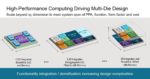
Artificial intelligence (AI) and machine learning (ML) are evolving at an extraordinary pace, powering advancements across industries. As models grow larger and more sophisticated, they require vast amounts of data to be processed in real-time. This demand puts pressure on the underlying hardware infrastructure, particularly… Read More
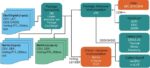
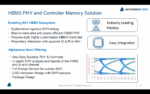
In the technology realm of artificial intelligence (AI) and high-performance computing (HPC), the demand for higher throughput and efficiency has never been greater. To meet these evolving demands, innovative memory solutions have emerged as critical enablers, paving the way for transformative advancements in computing… Read More
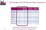
A quick Google search for “2.5D 3D IC” returns 669,000 results, so it’s a popular topic for the semiconductor industry, and there are plenty of decisions to make, like whether to use an organic substrate or silicon interposer for interconnect of heterogenous semiconductor die. Design teams using 2.5D and … Read More
The move to true 3D IC, monolithic 3D SOC and 3D heterogeneous integration may require one of the most major design tool architecture overhauls since IC design tools were first developed. While we have been taking steps toward 3DIC with 2.5D designs with interposers, HBM, etc., the fundamental tools and flows remain intact in many… Read More
On November 13, Cadence held its annual Photonics Summit. Cadence has been hosting this event for several years with the intention of advancing the photonics industry. With this event, Cadence has been a catalyst in furthering photonic product development. It’s quite remarkable that Cadence hosts such an event in a field where… Read More
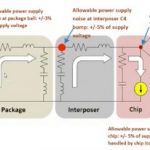
Innovations in packaging have played an important role in improving system performance and area utilization. Advances like 2.5D interposers and fan-out wafer-level packaging (FOWLP) have allowed mixed dies to be used in a single package and have dramatically reduced the number of connections that need to go all the way to the… Read More
The semiconductor industry has built decades of success on hyper-integration to increase functionality and performance while also reducing system cost. But the standard way to do this, to jam more and more functionality onto a single die, breaks down when some of the functions you want to integrate are built in different processes.… Read More
Dual in-line memory modules (DIMM’s ) with double data rate synchronous dynamic random access memory (DDR SDRAM) have been around since before we were worried about Y2K. Over the intervening years this format for provisioning memory has evolved from supporting DDR around 1995, to DDR1 in 2000, DDR2 in 2003, DDR4 in 2007 and DDR4… Read More