
While I missed ANSYS (and indeed everyone else) at DAC this year, I was able to attend the ANSYS Innovation Conference last week at the Santa Clara Convention Center. My primary purpose for being there was to listen to a talk by eSilicon which I’ll get to shortly, but before that I sat through a very interesting presentation on the growing importance of simulation in validating medical devices. This isn’t the kind of simulation we usually discuss; these are computational fluid dynamics (CFD) sims for blood flow through stents, insulin flow from insulin pumps and other such worthy objectives. ANSYS has a representative on an FDA advisory committee exploring increased use of simulations in regulation for medical devices. Important and fascinating stuff and a reminder of how broadly ANSYS impacts technology in many areas beyond electronic design.
Back to the main topic, eSilicon gave a presentation at the conference on their work with ANSYS to validate signal and power integrity in designs for eSilicon customers. You should understand first that eSilicon works with customers on the leading-edge of custom ASIC design, from HPC to networking, AI and 5G infrastructure. I wrote recently about their platform-specific offerings for AI and networking at 7nm in advanced 2.5D packaging options with high-bandwidth memory stacks. Point being that this is bleeding-edge design for system customers demanding total system performance, not just “the chip works to spec”. So, these designs are a good test for the ANSYS “chip-package-system” (CPS) mantra.
eSilicon doesn’t build the boards. Their customers do that, so they work collaboratively to extract, analyze and optimize the board design together with the ASIC package, interposer and components on the interposer. The speaker, Teddy Lee from eSilicon, detailed flows they used for signal integrity (SI), DC power integrity (PI) and AC power integrity. For signal integrity they extract 3D models from the MCM database into the ANSYS HFSS tool and from this build S-parameter models for insertion loss, return loss and crosstalk, then optimize traces, materials, spacing, etc. and iterate. They do this for the substrate layout and the interposer design, then connect the 2 models and send to the customer for use in their IBIS-AMI channel analysis.
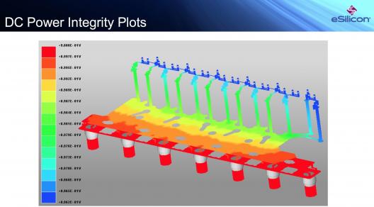
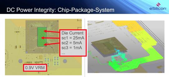
In DC power integrity, customers want to model DC voltage drop from the voltage regulator module (VRM) on the board, through trace and then through the package. Here a customer will again use SIwave to build a model, with IR drop and current densities, which eSilicon combines with a similar model extracted from the package substrate and the silicon interposer and then runs a DC simulation with SIwave. You can see simulated voltage gradients from the VRM to the package in the first figure and from the substrate up through the interposer in the picture above. This clearly provides very fine-grained analysis of power distribution all the way from the voltage regulator on the board up to the die ports.
In Teddy’s view, this system to die view, with accurate extraction at all levels, is essential to getting reliable PI analysis down to the die. He noted that you can’t just assume an idealized VRM somewhere on the PCB. You have to define where it’s going to sit and extract the real traces though which it will ultimately drive the package – the PI analysis you get from the idealized model may be quite different from the real model.
Teddy wrapped up with an explanation of their approach to AC power integrity where they want to look at the impact of noise generated by the die or on the board (everything looks good at DC, but what happens when a power domain turns on or another device on the board suddenly becomes active?). Here they use RedHawk to build a chip power model for the die and interposer, then combine that with an SIwave model for the package substrate and board. Based on this they do a system-level simulation (PCB down to the die) and perform a frequency domain simulation to see where they should add package-level decaps to reduce system-level resonances at the package. This is followed by a time-domain analysis looking at noise on the die. Depending on how this turns out, they may feed that back to the frequency domain analysis where they can change some of those decaps or perhaps change some trace geometries. And again iterate.
So, it looks like eSilicon sees value in CPS-style iterative analysis for SI and PI, given the demanding expectations of their customers. Chalk up another proof-point for CPS. You can learn more about CPS analysis HERE.
Share this post via:


Comments
There are no comments yet.
You must register or log in to view/post comments.