The explosion in volume and consumption of data, fueled by industry trends in virtualization, networking, and computing among others, continues to push photonic solutions forward into leading positions. On Feb 2nd, I attended a panel by Ansys at DesignCon that brought together industry experts from Intel, GlobalFoundries, Nvidia, Cisco, and Ayar Labs for a dynamic and all-encompassing discussion on the current state, challenges, and future of photonic technology and ecosystem. James Pond, Distinguished Engineer at Ansys and former CTO of Lumerical, moderated the panel and started the discussion with a big-picture overview.
Silicon Photonics: A relentless pursuit for speed & efficiency

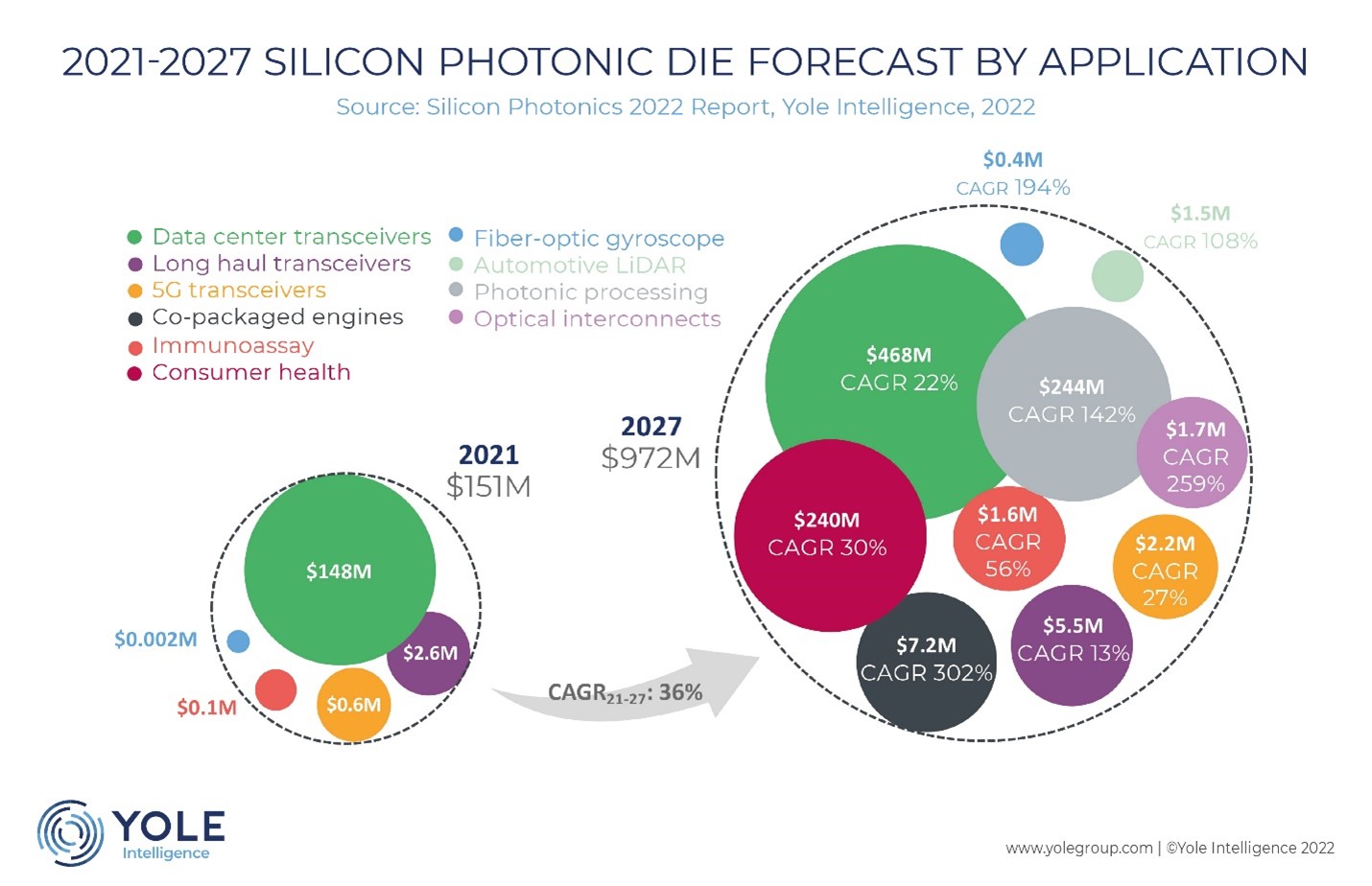
Faced with surging bandwidth demands and the related power being consumed by communications, the semiconductor industry is diversifying investments into optical interconnect technologies. Electrical interconnects are fundamentally limited in terms of scalability of performance, reach, and power consumption. This is where optical interconnects have the advantage. Analysts project 20% to 40% annual growth in the Silicon Photonics markets & applications over the next 5-10 years. While the growth to date has been largely driven by the datacom and transceiver markets, there is now exciting diversification of applications including LiDAR, bio-sensing, computing, new types of I/O, and quantum computing among many others.
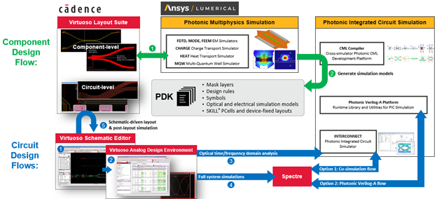
There is a genuine need for photonic systems and the industry has responded by creating an ecosystem closely resembling the electronic design automation (EDA) industry, commonly referred to as the electronic-photonic design automation (EPDA). The design tools and the overall ecosystem have come a long way from the early days when photonic PDKs (Process Design Kit) were solely offered as PDF files. A notable example is the advanced EPDA design tools as James Pond highlighted in figure 2, “Today we have the premier workflow in EPDA. It offers all kinds of things you would expect like schematic-driven layout, links & direct bridges between Virtuoso layout suite and Ansys multiphysics solvers, foundry-compatible customized design, parameter extractions to create accurate statistical compact models and support PDK development, and co-simulation to model entire systems accurately with both electronic and photonic compact models.”

The progress of the overall ecosystem enabled the first volume opportunity for integrated photonic products: the optical transceiver!
From Flexible Pluggable Transceivers to Co-packaged Optics Powerhouse
Today, photonics has already moved from dominance at kilometer-long distances down to meter-long distances. We saw pluggable photonic transceivers rapidly move from product introduction stages to producing multi-million units per year. Pluggable transceivers are highly modular and can be supplied by any vendor as long as they meet the targeted communication specifications. They are plugged directly into the front panel socket, then the signal is carried by electrical SerDes links to the ASIC where it can finally be computed and processed. The downside of this approach is that copper connections are susceptible to RF losses, especially when communicating at higher speeds. Robert Blum, Head of Silicon Photonics Strategy at Intel Foundry Services, recalled, “When we launched SiP in 2016 with pluggable transceivers, we also laid out a vision with the end goal of bringing optics to the processor. SiP is the only technology that can do that. The pluggable was a starting point and chip-to-chip optical links are expected to follow right on its heels.”
Faced with our insatiable appetite for data, the semiconductor industry is under pressure to keep up with even higher and higher bandwidth, latency, and power consumption demands which are pushing innovative solutions for moving the optics from the faceplate closer on-board and on-chip with the ASIC, completely eliminating the need for energy-sapping SerDes connections. “After much anticipation, in 2022, we started to see photonic solutions with fibers directly connecting into the ASIC packages instead of plugging into the faceplate. These are incredibly exciting times for photonics!”, commented Pond.
Now imagine we have the technology that breaks the speed and bandwidth limitations we have today! What would it mean to the architecture and the wide range of emerging applications in AI/ML? Matt Sysak, VP of laser engineering at Ayar Labs, describes a future of limitless possibilities, “If the assumptions that led to the way we design computers today change, it would mean having the freedom to re-imagine computer architectures. At Ayar Labs, we have a vision for optical I/Os everywhere which will not only accelerate computing but also potentially remake it.”
A Tale of two Technologies: Fundamental differences between electronics and photonics
On one hand, the rise of silicon photonics owes much of its success to capitalizing on the decades of investment in the electronics industry and the maturity of silicon wafer processing in CMOS manufacturing, Anthony Yu, VP of Silicon Photonics Product Management at GlobalFoundries further explained, “we continue to expand our photonics foundry capabilities to help our customers bring the advantages of photonics to different markets. We can only be successful if we apply the learning from our CMOS foundry model into photonics along with close collaboration across various parts of the ecosystem like the partnership with Ansys Lumerical to enable foundry compatible, predictable model libraries in PDKs.” Ashkan Seyedi, Silicon Photonics Product Architect at Nvidia added, “We look up to electronics as our big brother. Electronics gives us a benchmark to compare against so we know what maturity of PDKs and design workflows are necessary for a successful future in photonics technology.”
Yet, the consensus among all the panelists was that there are some fundamental differences between Electronics and Photonics, for one thing, there is no equivalent to Moore’s Law in SiP, at least not in the sense that we are doubling the density and halving the cost. Thierry Pinguet, Principal hardware engineer at Cisco and a seasoned veteran in photonics elaborated, “There is no equivalent to a transistor in photonics and thus no generational improvements from refining lithography to increase device density. The generational improvements in photonics come from innovation at component and circuit level design and assembly and packaging advancements.” This is why most silicon photonic platforms are based on older CMOS technology nodes.
Dennard scaling may have ended but the challenge remains, as the industry is facing unprecedented demands for high-speed networking/interconnects and accelerated computing. Pushed into uncharted territory where Moore’s law is truly struggling to stay on course, photonics offers the opportunity to keep that progress going. Seyedi proposed “it is time to redefine Moore’s law. When we zoom way out, the systems are continuously improving. We should consider new metrics by which Moore’s law extends, such as packaging.”
Regardless of how you define Moore’s law, there are inflection points where new photonic technologies are introduced. Today, data centers are using 800Gb products, but a couple of years ago it was 400 Gb and 200Gb before that. There have been several factors contributing to this scaling in the overall transmission capacity including higher-order modulation formats like quadrature amplitude modulation (QAM) enabled by advanced digital signal processing (DSP) techniques and massive parallelism such as wavelength-division multiplexing (WDM), as well as innovative designs at the component level such as segmented modulators. Given the fundamental trade-off between bandwidth and modulation efficiency linked to physical factors like the photon lifetime in silicon, designers are exploring heterogeneous integration of new materials on the front end. Future photonic solutions are also relying on advances in traditional 2.5D and 3D packaging in electronics but perhaps we’ll also come to see innovation in the photonic aspects of packaging such as fiber-to-chip wire bonding.
Lighting the path to scalability
Packaging was a hot topic that resonated with all the panelists and brought up the challenges around standardization and lack of IP in the ecosystem. Consider fiber attachment, which involves placing and gluing fibers into a package at precise locations where minimizing losses due to misalignment gets more challenging with the increasing number of fibers. There is much common knowledge gathered over the decades within the community around fiber attachment, but many designers still expend resources in developing their own process. “It just doesn’t add intrinsic value. Designers want to focus on innovating and not reinventing the wheel because there is no turnkey solution. Today, people are still innovating but we’re also starting to see some convergence in certain areas. This is why Intel came out with a small-form-factor, high-density detachable fiber connector that has compatible losses to other co-packaged optics approaches and is compatible with standard industry PIC and with any 2D, 2.5D, or 3D packaging. Standards and IP libraries are key components in the photonics ecosystem that are needed to make optics into a high-volume play.” said Blum.
Over the recent years we have started to see manufacturing players evolving to offer open-access models for prototyping, multi-project wafer runs for R&D, and low-to-high-volume throughput for those vendors ramping up for commercialization. Foundries are economically driven, which translates into maximizing consolidation into a single platform. “The challenge is that vendor differentiation in the photonics industry today isn’t based on a single platform with set pieces of IP blocks as exists in the ASIC world. At least not yet. If you open any pluggable module, they’ll look different inside as every solution is customized. Demanding applications requirements are driving the design of customized devices that likely won’t be offered under a single platform.” Pinguet explained. Sysak added, “There are many ways for an optical I/O technology to communicate with a processor but to truly take advantage of economies of scale, we need reliable and scalable manufacturing, and this is something we’re tackling together with GlobalFoundries.”
On the one hand, the silicon photonic ecosystem is advancing towards standardization of processes, platforms, and design automation, especially for established applications like pluggable transceivers. On the other hand, demands for higher performance and emerging new applications are driving customization and pushing for the introduction of new materials and processes. We are still in the early days. “In time we’ll see photonics move towards an ASIC-like model with IP providers and consolidated platforms which will enable high-volume solutions. But right now, we celebrate the creativity and brilliance of our photonic designers.” Yu summarized.
Learn more about challenges and solutions in Silicon photonics:
Photonic Simulation Software | Ansys
Design a Silicon Photonic Ring-Based WDM Transceiver with EPDA
Also Read:
Unlock First-Time-Right Complex Photonic Integrated Circuits
Whatever Happened to the Big 5G Airport Controversy? Plus A Look To The Future
Ansys’ Emergence as a Tier 1 EDA Player— and What That Means for 3D-IC
Share this post via:


Comments
There are no comments yet.
You must register or log in to view/post comments.