

Over its 40+ year history, electronic design automation (EDA) has seen many companies rise, fall, and merge. In the beginning, in the 1980s, the industry was dominated by what came to be known as the big three — Daisy Systems, Mentor Graphics, and Valid Logic (the infamous “DMV”). The Big 3 has morphed over the years, eventually settling in for a lengthy run as Cadence, Synopsys, and Mentor. According to my friend, Wally Rhines’ always informative presentations, the Big 3 have traditionally represented over 80% of the total EDA revenue. However, EDA is now absolutely led by four major billion-dollar-plus players, plus a collection of much smaller niche suppliers. The “Big 3” is now the “Big 4,” consisting of Ansys, a $2 billion Fortune 500 company, Synopsys, Cadence Design Systems, and Siemens Digital Industries Software (née Mentor Graphics). Much smaller, niche players like Silvaco (the next largest) follow in the distance with a cool $50 million in revenues.
Ansys has a 50-year history in engineering simulation, but its involvement in EDA began just with the acquisition of Apache in 2011. In the process, Ansys acquired Redhawk — a verification platform specifically for the power integrity and reliability of complex ICs, along with a suite of related products that included Totem, Pathfinder and PowerArtist. This evolution continued with the acquisition of Helic with its suite of on-chip electromagnetic verification tools, and subsequent acquisitions in domains such as photonics, to address key verification issues in IC development.
To give context to Ansys’ role in the current EDA ecosystem, the chip design flow consists of 40 or more individual steps executed by a wide range of software tools. No single company can hope to cover the entire flow. While every stage is important, there are certain extremely difficult, critical verification steps mandated by semiconductor manufacturers that all chips must pass. These signoff verifications are required before foundries will accept a design for manufacture.

Referred to as golden signoff, they include:
- Design Rule Checking (DRC)
- Layout vs. Schematic (LVS)
- Timing Signoff (STA: static timing analysis)
- Power Integrity Signoff (EM/IR: electromigration/voltage drop).
The reliability and confidence in these checks rests on industry reputations and experience built up over decades, including years of close collaboration with foundries, which makes golden signoff tools very difficult and risky to displace. Today, virtually every IC design relies on Calibre from Siemens and PrimeTime from Synopsys. Joining these two longstanding golden tools, Ansys RedHawk-SC™ (for digital design) and Ansys Totem (for analog/mixed signal (AMS) design) are golden tools for power integrity signoff, critical for today’s advanced semiconductor designs.
Foundry Certification
Beyond the signoff certification of RedHawk-SC and Totem for power integrity, other Ansys tools have also been qualified by the foundries for a range of verification steps including on-chip electromagnetic modeling (RaptorX, Exalto, VeloceRF), chip thermal analysis (RedHawk-SC Electrothermal), and package thermal analysis (Icepak).
Due to limited engineering resources and demanding schedules, foundries typically work with just a few select EDA vendors as they develop each new generation of silicon processes. Most of these collaborations now exist within the bubble of the Big 4, hinging on relationships built on a reputation for delivering specific technological capabilities, working relationships forged over many years, and the reliability of those tools established by working with a wide spectrum of customers over many technology generations.
Ansys Brings EDA Into the 3D Multiphysics Workflow
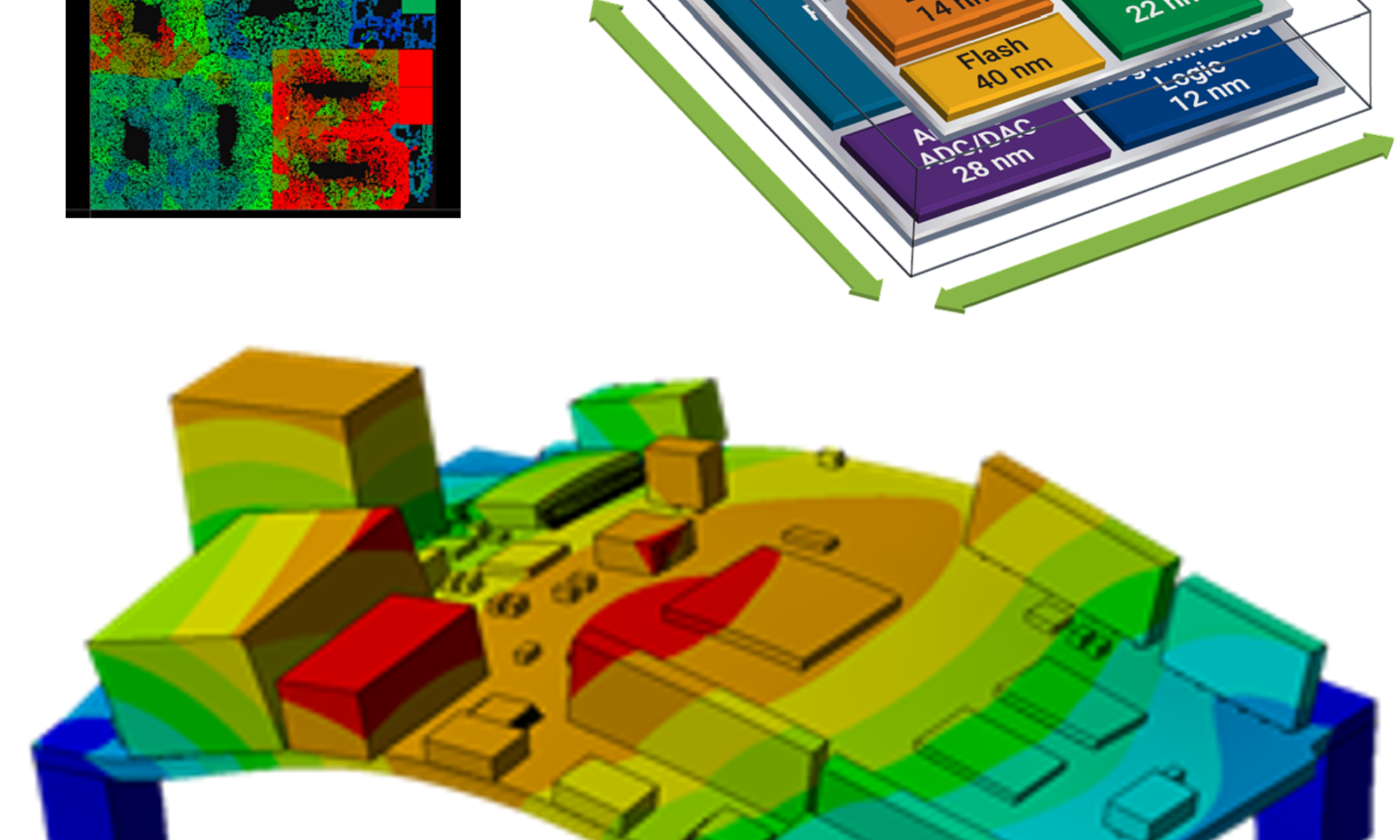
The evolution of semiconductor design is moving beyond scaling down to ever-smaller feature sizes and is now addressing the interdependent system challenges of 2.5D (side-by-side) and 3D (stacked) integrated circuits (3D-IC). These disintegrate traditional monolithic designs into a set of ‘chiplets’ that offer benefits in yield, scale, flexibility, reuse, and heterogenous process technologies. But in order to access these advantages, 3D-IC designers must grapple with the significant increase in complexity that comes with multi-chip design. Many more physical effects must be analyzed and controlled than in traditional single-chip designs, and a broad suite of physical simulation and analysis tools is critical to manage the added complexity of the multiphysics involved.
Ansys has strategically positioned itself to take on these challenges as an industry leader by leveraging its lengthy, broad multiphysics simulation experience with updated Redhawk-SC and Totem capabilities to support advances in power integrity for 3D-IC. This includes brand new capabilities like RedHawk-SC Electrothermal that are targeted specifically at 3D-IC design challenges with thermal and high-speed integrity.
Over the past few years, Ansys has been recognized by TSMC for its critical role in the EDA design flow. In 2020, Ansys achieved early certification of its advanced semiconductor design solution for TSMC’s high-speed CoWos (Chip-on-Wafer-on-Substrate) design, and InFO (Integrated Fan-Out) 2.5D and 3D packaging technologies. Continued successful collaboration with TSMC has delivered an hierarchical thermal analysis solution for 3D-IC design. In a more recent collaboration, Ansys Redhawk-SC and Totem achieved signoff certification for TSMC’s newest N3E and N4P process technologies. Similar collaborations for advanced processes, multi-die advanced packaging, and high-speed design have led to certifications from Samsung and GlobalFoundries. Ansys is even moving beyond foundry signoff and certification to define reference flows incorporating these tools, such as TSMC’s N6 radio frequency (RF) design reference flow.
TSMC has also recognized Ansys with multiple Partner of the Year Awards in the past 5 years, most recently in:
- Joint Development of 4nm Design Infrastructure for delivering foundry-certified, state-of-the-art power integrity and reliability signoff verification tools for TSMC N4 process
- Joint Development of 3DFabric™ Design Solution for providing foundry-certified thermal, power integrity, and reliability solutions for TSMC 3DFabric™, a comprehensive family of 3D silicon stacking and advanced packaging technologies
Achieving Greater Efficiency through Engineering Workflows
As more system companies embark on designing their own bespoke silicon and 3D-IC technology becomes more pervasive, more physics must be analyzed, and they must be analyzed concurrently, not in isolation. Multiphysics is not merely multiple physics. Building a system with several closely integrated chiplets is more complex, so more physical/electrical issues come into play. In response, Keysight, Synopsys and others have chosen to partner with Ansys, recognizing the value of its open and extensible multiphysics platforms. Keysight has integrated Ansys HFSS into their RF flow, while Synopsys has tightly integrated Ansys tools into their IC design flow.
Ansys is well-positioned to accelerate 3D-IC system design, offering essential expertise in different disciplines — in EDA and beyond — for an efficient workflow that spans a range of physics in virtually any field of engineering. For example, Ansys solutions support the complete thermal analysis of a 3D systems, including the application of computational fluid dynamics to capture the influence of cooling fans, and mechanical stress/warpage analysis to ensure system reliability despite differential thermal expansion of the multiple chips. Ansys even provides technology to address manufacturing reliability, predicting when a chip will fail in the field. These products enable the understanding of silicon and systems engineering workflows from start to finish.
Ansys’ influence as a leader in physics spans decades. It extends beyond multiple physics to multiphysics-based solutions that consider interactions more consistent with 3D-IC systems development simultaneously — in thermal analysis, computational fluid dynamics for cooling, mechanical, electromagnetic analysis of high-speed signals, low-frequency power oscillations between components, safety verification, and more, all within the context of the leading EDA flows. And, Ansys’ open and extensible analysis ecosystem connects to other EDA tools and the wider world of computer-aided design (CAD), manufacturing, and engineering.
Summary
There’s little doubt that 3D-IC innovation is accelerating. As systems companies expand further into 3D-IC, they will continue to look to, and trust Ansys solutions in support of their IC designs. To date, the vast majority of the world’s chip designers rely on Ansys products for accurate power integrity analysis. Ansys provides cyber-physical product expertise, with an acute understanding of silicon and system engineering workflows. With one foot in the semiconductor world, and another in the wider system engineering world, Ansys is uniquely positioned to provide broader multiphysics solutions for 2.5D/3D-IC that will continue to grow its footprint in EDA. The EDA Big 3 is now the Big 4, absolutely.
Also Read:
WEBINAR: Design and Verify State-of-the-Art RFICs using Synopsys / Ansys Custom Design Flow
What Quantum Means for Electronic Design Automation
The Lines Are Blurring Between System and Silicon. You’re Not Ready.
Share this post via:


Comments
There are no comments yet.
You must register or log in to view/post comments.