

IEDM is in my opinion the premiere conference for information on state-of-the-art semiconductor processes. In “My Top Three Reasons to Attend IEDM 2019” article I singled out the TSMC 5nm paper as a key reason to attend.
IEDM is one of the best organized conferences I attend and as soon as you pick up your badge you are handed a memory stick with all the conference papers (unlike some other conferences where there are no proceedings). It is very useful to get the papers before seeing them, I typically review a paper, see it presented, and then review it again. I quickly previewed the TSMC paper in advance of the presentation and I have to say I was very disappointed with the lack of real data in the paper, there were no pitches and most of the results graphs were in normalized units. At the 2017 IEDM conference Intel and GLOBALFOUNDRIES (GF) presented their 10nm (7nm foundry equivalent) and 7nm processes respectively and both companies provided critical pitches and electrical results in real units. You can see my previous write up on these papers here.
I would like to take this opportunity to call on TSMC to provide more transparency with respect to their processes.
At the press lunch on Monday many of the IEDM session chairs were available and I asked them about this paper and whether they ever push back on companies to provide more data or reject a paper for lacking enough detail. The answer I got back was yes and in fact they turned down a platform paper from another leading logic company this year for lack of data and said they debated whether to let the TSMC paper in. It is a difficult position for the organizers, this is the kind of headline paper that attracts attendees but at the same time the conference must maintain a standard of quality.
In the balance of this article I will discuss what TSMC disclosed and then try to fill in some of the details they didn’t disclose based on my own investigations. I have read the paper, seen the paper presented, and asked the presenter a question at the end of the presentation and discussed this process with a wide range of industry experts.
TSMC’s disclosures
The key bullet points from the TSMC paper and presentation are:
- Industry leading 5nm process.
- Full fledged EUV, >10 EUV layers replacing >3 immersion layers each resulting in a reduction in mask count improving cycle time and yield. The paper says >4 immersion layers for each EUV layer but in the presentation the presenter said >3.
- High mobility channel FETs.
- 021µm2 high density SRAM.
- ~1.84x logic density improvement, ~1.35x SRAM density improvement and ~1.3x analog density improvement.
- Gate contact over diffusion, unique diffusion termination, EUV based gate patterning for logic and SRAM.
- ~15% speed gain or 30% power reduction.
- Low resistance and capacitance interconnect with enhanced barrier lines and etch stop layer (ESL) with copper reflow gap fill. The Back-End-Of-Line (BEOL) also features a high resistance resistor for analog use and super high-density Metal-Insulator-Metal (MIM) capacitors
- 5 and 1.2 volt I/O transistors.
- True multi-threshold voltage process with 7 threshold voltages over a >250mv range supported and an extreme low Vt transistor 25% faster than the previous generation. Presumably only around 4Vts are available at a time.
- Passed qualification.
- High yielding test chip with 256Mb SRAM and CPU/GPU/SOC blocks and D0 ahead of plan with a faster yield ramp than any previous process. 512Mb SRAM has ~80% average yield and >90% peak yield.
- In risk production now with 1st half 2020 planned high volume production.
Density and pitches
At 7nm Samsung and TSMC have similar process densities. Moving from 7nm to 5nm Samsung has disclosed a 1.33x density improvement and TSMC has disclosed a ~1.84x density improvement. Clearly TSMC will have a far denser process than Samsung and with Intel’s 7nm (5nm foundry equivalent process) not due until 2021, TSMC will have the process density lead in 2020.
In terms of specifics other than an SRAM cell size of 0.021µm2 TSMC didn’t provide any. SRAM density is certainly important for SOC designs where SRAM can often make up over half the device area.
Logic designs are created with standard cells. The height of a standard cell is the Metal 2 Pitch (M2P) multiplied by the track height (TH) and the width is defined by the Contacted Poly Pitch (CPP), cell type and whether the process supports single or double diffusion break. For the TSMC 7FF process M2P is 40nm and the TH is 6. The CPP is specified as 54nm although 57nm is seen in standard cells, however since TSMC stated their density improvement we will assume 54nm as a starting point and the process supports a double diffusion break (DDB). Running these dimensions through the Intel density metric we have discussed before yields 101.85 million transistor/mm2.
I have heard that TSMC is going to use a very aggressive 28nm M2P at 5nm and I also believe they will stay with a 6-track cell. A 5-track cell requires Buried Power Rails (BPR) and TSMC did not disclose that as part of the process, I also believe it is too early to see BPR in a process. I also expect this process to support Single Diffusion Break (SDB), SDB was added with the 7FFP version of TSMC’s 7nm process and I believe they will maintain that. The net result is for a 1.84 density improvement CPP is between 49 and 50nm. If I assume 50nm I get 185.46 MTx/mm2 a 1.82x improvement in density.
Figure 1 presents a 7FF versus 5FF process comparison.
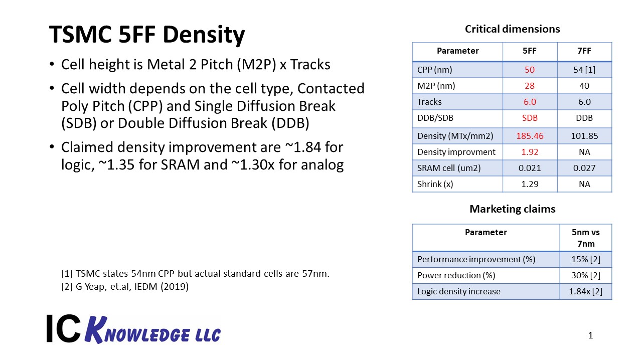
Figure 1. TSMC 5FF Process Density.
EUV usage
As I stated previously, the paper mentions a single EUV layer replaces >4 immersion layers although the presentation revised this to >3 immersion layers. The paper and presentation both report 5nm using >10 EUV layers and that would imply >30 immersion layers will be replaced. This is presumably versus the number of immersion layers required if 5FF were done with multi patterning instead of with EUV.
In the article a graph of mask layers is presented with normalized units where 16FFC is 1.00, 10FF ~1.30, 7FF ~1.44 and 5FF ~1.30. I believe TSMC’s 7FF process is 78 masks and the 5FF is 70 masks. When I use my mask estimates for 16FFC, 10FF, 7FF and 5FF I reproduce the graph from the paper nicely.
I also believe TSMC’s 7FFP process has ~5 EUV masks and 5FF will have ~15 EUV masks.
Another interesting EUV comment, I am hearing Samsung has a very high dose for their EUV process for critical layers and I have heard TSMC’s EUV dose is much lower with TSMC a >2x throughput advantage over Samsung> This is also consistent with reports that Samsung is having trouble getting enough wafers through their EUV tools. At another conference I saw an IBM presentation where they discussed developing the 5nm process with Samsung. They said that they turned up the EUV dose until they got good yield and transferred the process to Samsung with the idea that Samsung would then work on reducing the dose. It sounds like the process may have been rushed into production before reducing the EUV dose.
High mobility channels
I have been expecting for some time that Silicon Germanium (SiGe) High Mobility Channels (HMC) will be introduced at 5nm for pFETs.
When I got the TSMC paper and read through it they talk about HMCs plural and even have a figure that says HMC and show both nFET and pFET results, they further show HBC on silicon with no interface buffer layers. The only answer that fits this in my view would be if TSMC had implemented Germanium channels for both nFET and pFET devices, but I thought that was an advance that wasn’t ready yet. If that were the case this would be similar to Intel introducing High K Metal Gates (HKMG) at 45nm or FinFETs at 22nm.
After the TSMC talk I asked the presenter whether the nFET and pFET devices were both HHC or just the nFET or just the pFET. The presenter responded that only one of the device types had HMC although he wouldn’t say which one. I believe it is almost certain that the pFET is a SiGe channel as expected.
Conclusion
In conclusion TSMC has developed a high density 5nm process that will provide the industries highest process density in 2020 and establishes TSMC as the current leader in logic process technology.


Comments
10 Replies to “IEDM 2019 – TSMC 5nm Process”
You must register or log in to view/post comments.