At the risk of highlighting my abundant lack of expertise in the domain, I had always viewed EMC (electromagnetic compatibility) compliance and testing as one of those back-end exercises that can only be done on the real device and depends on a combination of expertise and brute-force in chip/package/module/system design (decaps, etc) to ensure a reasonable chance of passing. One site I found has some interesting stats in this area, suggesting first time pass-rates of only 50%, and rather lax enforcement in practice for non-wireless devices, indicating that getting to compliance is not trivial, nor has it been considered especially important, at least by a significant number of vendors.

However it seems this is likely to change. As devices move into much more safety critical applications, particularly in cars, expectations are rising. Not only is there likely to be a high and more strictly enforced requirement that applications (including non-wireless devices) will not interfere with other external electronics, but also testing for immunity of the device itself to external interference is becoming more sophisticated. The FCC has announced new rules requiring EMC testing to be done only by accredited labs with the resources and equipment to meet these needs, a factor which apparently is driving significant consolidation among labs to get to this new critical mass.
So, more rigorous and more expensive testing, together with more rigorous enforcement and potentially significant fines for non-compliance. In advanced technologies running at higher frequencies, more help to design for compliance will probably be welcome. ANSYS recently hosted a webinar in which Professor Nagata of Kobe University presented the work they are doing, together with Toshiba and ANSYS, to explore methods to design for and simulate for compliance while still at the design stage. Simulation is supported by the ANSYS RedHawk and HFSS among others.
They are particularly looking at effects of interference, both internal and external, in LTE subsystems, for example in V2x applications. Here, noise can come both from internal circuitry, the regular power noise as functions in the chip become active or inactive, as well as the noise from switching power domains that are common in many low-power applications today.
They attack both components of EMC – electromagnetic interference (EMI) generated by the application, and electromagnetic susceptibility (EMS) to external interference – using the ANSYS tools. I am not going to attempt to replay the level of detail Professor Nagata goes into; you can watch the webinar replay for a closer understanding. The main top-level points I saw are that:
- They use both passive models for the chip, package and system in their response model, and active models for the ESD devices at the chip I/Os. Their comparison of simulations based on this approach with measured response curves show good correspondence, so I’m sold that the methodology is robust.
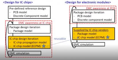
- Analysis starts by building EMC awareness at chip design, supported by a reference PCB model. They then iterate from package design and model through IC design based on a chip power model (CPM). The EMI component of this Professor Nagata considers fairly straightforward. He says that EMS analysis is not so easy since this needs to account for non-linearity in the ESD devices in response to potentially Watts of external signal. To deal with this they use an extended CPM model to include the active (non-linear) behavior
- One the chip model is optimized, they pass this extended CPM model over to the PCB analysis team to support their compliance modeling, again an iterative process to optimize for and effective while managed-cost solution.
Professor Nagata did note that their work is still at the research phase, but it seems quite promising already. Building EMC compliance analysis into the chip, package and system phases of design sounds like a better way to converge on successful certification against these new regulatory requirements. You can register to watch the webinar HERE.
Share this post via:


Comments
There are no comments yet.
You must register or log in to view/post comments.