You are currently viewing SemiWiki as a guest which gives you limited access to the site. To view blog comments and experience other SemiWiki features you must be a registered member. Registration is fast, simple, and absolutely free so please,
join our community today!
            WP_Term Object
(
    [term_id] => 159
    [name] => Siemens EDA
    [slug] => siemens-eda
    [term_group] => 0
    [term_taxonomy_id] => 159
    [taxonomy] => category
    [description] =>
    [parent] => 157
    [count] => 717
    [filter] => raw
    [cat_ID] => 159
    [category_count] => 717
    [category_description] =>
    [cat_name] => Siemens EDA
    [category_nicename] => siemens-eda
    [category_parent] => 157
    [is_post] =>
)

WP_Term Object
(
    [term_id] => 159
    [name] => Siemens EDA
    [slug] => siemens-eda
    [term_group] => 0
    [term_taxonomy_id] => 159
    [taxonomy] => category
    [description] =>
    [parent] => 157
    [count] => 717
    [filter] => raw
    [cat_ID] => 159
    [category_count] => 717
    [category_description] =>
    [cat_name] => Siemens EDA
    [category_nicename] => siemens-eda
    [category_parent] => 157
    [is_post] =>
)
Design For Manufacturing (DFM) is the art and science of making an IC design yield better in order to receive a higher ROI. Ian Smith, an AE from Mentor in the Calibre group presented a pertinent webinar, IP Scoring Using TSMC DFM Kits. I’ll provide an overview of what I learned at this webinar.… Read More
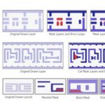
Double patterning at 20nm is one of those big unavoidable changes that it is almost impossible to know too much about. Mentor’s David Abercrombie, DFM Program Manager for Calibre, has written a series of articles detailing the multifaceted impacts of double patterning on advanced node design and verification. There is… Read More
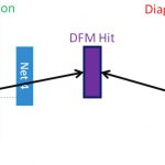
Sign up for a free webinar on December 11 on Accelerating Yield and Failure Analysis with Diagnosis.
The one hour presentation will be delivered via webcast by Geir Eide, Mentor’s foremost expert in yield learning. He will cover scan diagnosis, a software-based technique, that effectively identifies defects in digital logic… Read More
Wanna become the double patterning guru at your company? David Abercrombie, DFM Program Manager for Calibre, has written a series of articles detailing the multifaceted impacts of double patterning on advanced node design and verification. For designers struggling to understand the complexity and nuances of double patterning,… Read More
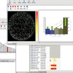
Since the beginning of the semiconductor industry, improving the rate of yield learning has been a critical factor in the success silicon manufacturing. Each fab has dedicated yield teams that look at the yield of wafers manufactured the previous day and attempt to find the root cause of any unexpected “excursions.” In earlier… Read More
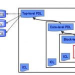
The creation of test patterns for mixed signal IP has been, to a large extent, a manual effort. To improve the process used to test, access, and control embedded IP, a new IEEE P1687 standard is being defined by a broad coalition of IP vendors, IP users, major ATE companies, and all three major EDA vendors. This new standard, also called… Read More
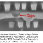
Finding and debugging failures on integrated circuits has become increasingly difficult. Two sessions at ISTFA (International Symposium for Testing and Failure Analysis) on Thursday address the current best practices and research directions of diagnosis.
The first was a tutorial this morning by Mentor Graphics luminary… Read More
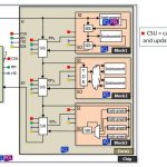
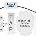
Until now, the integration and testing of IP blocks used in large SOCs has been a manual, time consuming design effort. A new standard called IEEE P1687 (or “IJTAG”) for IP plug-and-play integration is emerging to simplify these tasks. EDA tools are also emerging to support the new standard. Last week mentor announcedTessent IJTAG,… Read More
Test is the Rodney Dangerfield of EDA, it doesn’t get any respect. All designs need to be tested but somehow synthesis, routing, analog layout and the rest are the sexy areas. In my spoof all purpose EDA keynote address I even dissed it:You are short on time so slip in a quick mention of manufacturing test. Who knows anything … Read More
Most of us live perfectly good lives without distinction, fame, or note. Others rack up the honors, filling their walls and resumes with recognition of their brilliance. Like Dr. Janusz Rajski.
Rajski is the director of engineering for the test products at Mentor Graphics, an IEEE Fellow, and the inventor of embedded deterministic… Read More