 Design For Manufacturing (DFM) is the art and science of making an IC design yield better in order to receive a higher ROI. Ian Smith, an AE from Mentor in the Calibre group presented a pertinent webinar, IP Scoring Using TSMC DFM Kits. I’ll provide an overview of what I learned at this webinar.
IP DFM Metrics
Random and systematic silicon defects in IC layout can be categorized and measured in several ways:
- Chemical Mechanical Polishing (CMP)
- Critical Area Analysis (CAA)
- Critical Feature Analysis (CFA)
- Litho Process Check (LPC)
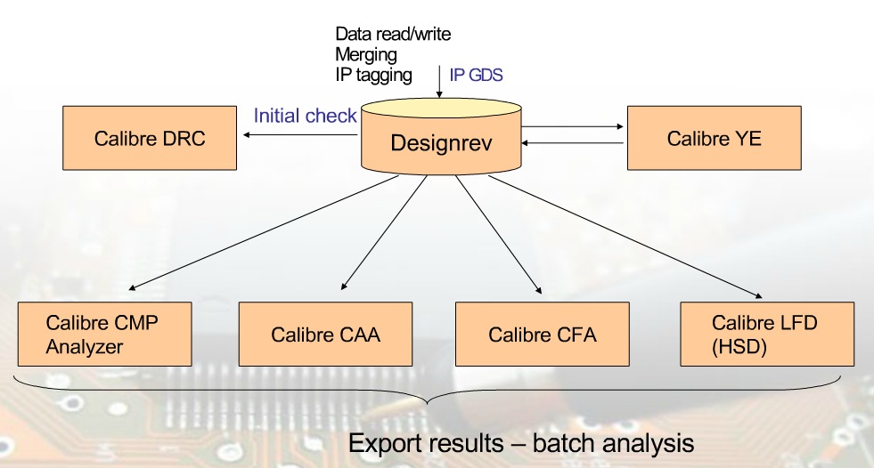
With the Calibre tools you can run these four types of DFM analysis from a GUI called Designrev:
CMPA
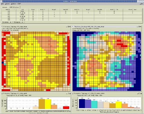
This type of analysis shows how planar the IC layout surface is, and the density. Copper interconnect dishing or oxide erosion can cause metal to bridge, creating a short circuit defect. Depth of focus measurement is important during the lithography process and can be viewed graphically for Metal 3 before (right) and after (left) CMPA:
CAA
If there is a processing defect present on your IC layout, then how sensitive is your IP to an open or a short? Every fab has a defect probability based on defect size for all layers:
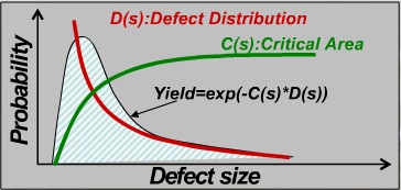
If you take that defect probably information and apply it to your IP layout, then you can determine how sensitive the layout is to opens and shorts:

Shown in grey on the left-hand layout are all the areas where a defect would cause a short circuit, while the dark green areas on the right-hand layout are the areas where a defect would cause an open circuit.
The fab keeps the defect probability low, while it’s up to the IC designer to minimize the Critical Areas reported in CAA.
LPC
Litho simulation checks for hot-spots in the IC layout to identify failures like metal necking:
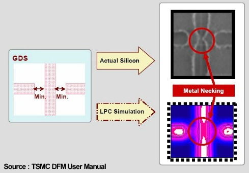
During IC fabrication a light source is used to expose the interconnect and transistor patterns. The LPC simulation uses the Dose and Focus characteristics of the light source to predict how silicon will actually be realized:

The colored lines on the LFD simulation are bands that show the shape variation of an IC layer. By pinpointing these hot-spots the IC designer can take corrective action.
CFA
Design rules from the fab have a distribution as shown in the following curve of Yield as a function of spacing:
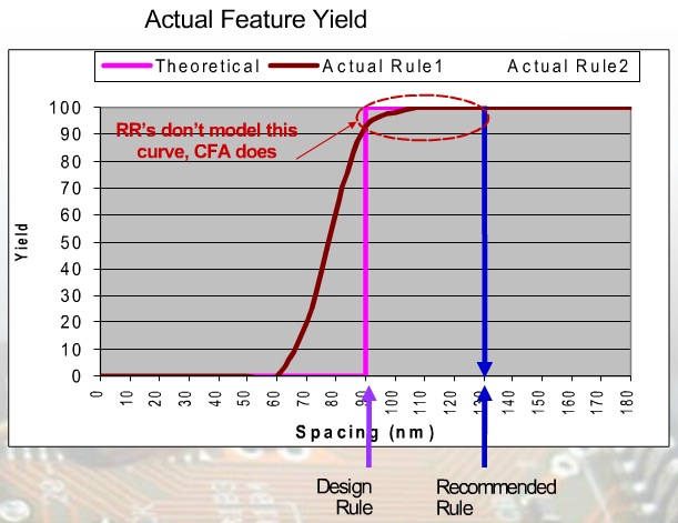
By running CFA analysis the IC designer can get feedback on areas that will lower yield. There’s even automation to add polygons to your layout to make it comply to the Recommended Rule.
Implementing a DFM Flow
- Score your new IP with DFM analysis tools and give it a score
- Correlate actual silicon failures with DFM predicted measurements
- Create a yield learning database to Verify, Analyze and Correlate defects
- Tag all IP with historic info
Here’s an IC design library with 27 different IP blocks analyzed with CAA and the results shown on a Predicted Random Defect Yield chart for opens / shorts / Via issues:
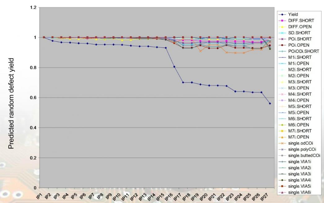
The Y-axis is a predicted random yield, then X-axis has each IP block in the library. The blue line is the cumulative yield for the library. Several cells (IP16 to IP27) show a significant yield drop based on this analysis and should be fixed.
Test Diagnostics and Analysis
DFT tools used in Failure Analysis (FA) can measure actual silicon failures and then pinpoint them on the IC layout, finding the actual cell or net.
Link to Layout
Silicon test reports have identified a short circuit between two internal nets of an IC as shown in the upper-left corner:
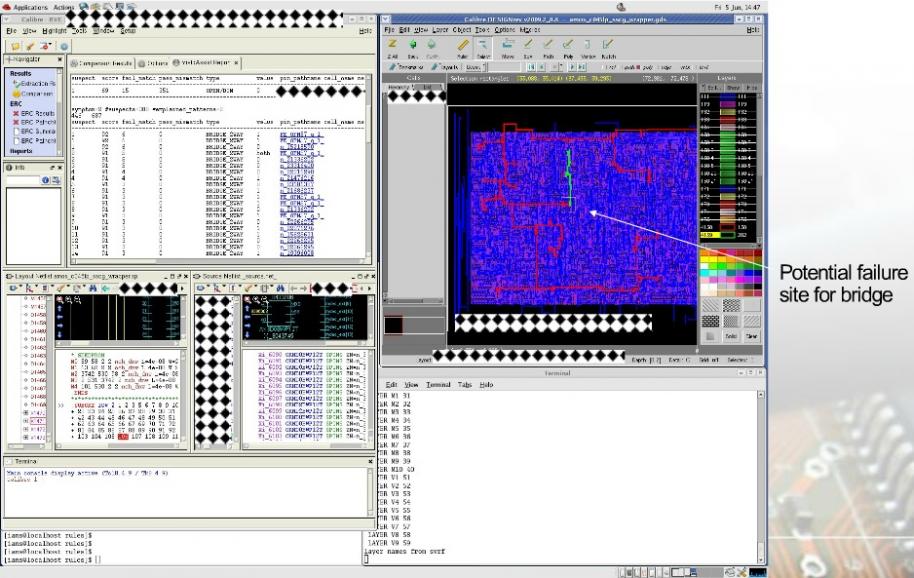
Below that are the schematic and layout netlist comparison windows, in the lower-left corner.
Finally on the right-hand side is the actual IC layout with the two nets highlighted in Red and Blue colors. The white arrow pinpoints the likely failure location causing the short circuit.
Zooming into the potential failure site you can see likely causes of the bridge defect:
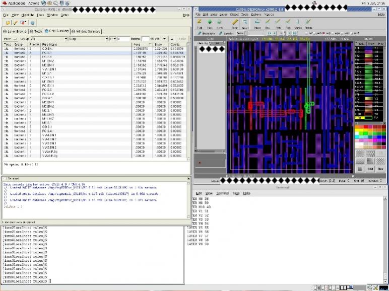
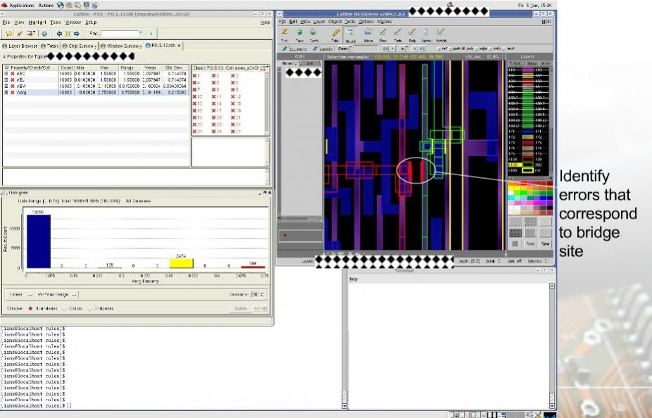
Highlighted in Red color is a rule for Poly Space recommended rule. By loading the DFM result error database and comparing that to the best/worst compliance we can identify errors that correspond to the bridge site shown by red bars:
Summary
DFM analysis can be used to score IP blocks and improve yields, you can actually screen IP block and standard cells for DFM quality before tape-out, silicon failure analysis can be correlated to DFM measurement, and DFT tools can be directed by DFM analysis of layout to find low-yield layout areas.
IC designers must be involved with thinking about improving yield before tape-out, and now they have some tools and a methodology to do this.
Share this post via:


Comments
There are no comments yet.
You must register or log in to view/post comments.