You are currently viewing SemiWiki as a guest which gives you limited access to the site. To view blog comments and experience other SemiWiki features you must be a registered member. Registration is fast, simple, and absolutely free so please,
join our community today!
The semiconductor industry has achieved extraordinary mastery in silicon signoff. Modern EDA environments can now optimize timing closure, physical verification, IR/EM behavior, routing density, thermal interaction, and increasingly even design-space exploration through AI-assisted implementation flows. Crossing… Read More
Siemens has strengthened its position in EDA and manufacturing by acquiring ASTER Technologies, a specialist in test and reliability solutions for printed circuit boards. The acquisition represents a strategic step in Siemens’ broader vision to deliver a fully integrated, end-to-end digital thread for electronics design,… Read More
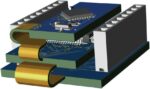
From Zion Research I learned that the flexible electronics market was about $13.2B in 2021 and growing at a CAGR of 21%, so that was impressive. There are several factors that make rigid-flex circuit so attractive, like: space efficiency, reduced weight, enhanced reliability, improved signal integrity, streamlined assembly,… Read More
I first met Jimmy Chen from Easy-Logic at #60DAC and wrote about their Engineering Change Order (ECO) tool in August 2023. Recently we had a Zoom call so that I could see a live demo of their EDA tool in action. Allen Guo, the AE Manager for Easy-Logic gave me an overview presentation of the company and some history to provide a bit of context.… Read More
Power management integrated circuits (PMICs) are integrated circuits for power management. Driven by the strong demand in consumer electronics, IoT, and the automobile industry, the design for PMIC is getting more challenging in terms of integration, reliability and efficiency. The design methodology needs to be updated… Read More
Humans certainly have always had an aesthetic preference for symmetry. We also see symmetry showing up frequently in nature. The importance of symmetry in electronic designs has been apparent for decades. There are a host of analog structures that require balanced layout. For instance, these include differential pairs and … Read More
A decade ago, many of us heard commentaries on how entrepreneurs were turned down by venture capitalists for not including a cloud strategy in their business plan, no matter what the core business was. Humorous punchlines such as, “It’s cloudy without any clouds” and “Add some cloud to your strategy and your future will be bright… Read More
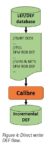
GDS and LEF/DEF each came about to support data exchange in different types of design flows, custom layout and place & route respectively. GDS (or stream format) was first created in the late 1970s to support the first generation of custom IC layout tools, such as Calma’s GDSII system. Of course, the GDS format has been updated… Read More
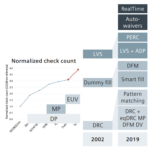
Physical verification is an important and necessary step in the process to tapeout an IC design, and the foundries define sign-off qualification steps for:
- Physical validation
- Circuit validation
- Reliability verification
This sounds quite reasonable until you actually go through the steps only to discover that some of the … Read More
There is an emerging set of advanced packaging technologies that enables unique product designs, with the capability to integrate multiple die, from potentially heterogeneous technologies. These “system-in-package” (SiP) offerings provide architects with the opportunity to optimize product performance, power, cost,… Read More