You are currently viewing SemiWiki as a guest which gives you limited access to the site. To view blog comments and experience other SemiWiki features you must be a registered member. Registration is fast, simple, and absolutely free so please,
join our community today!
Technology trends make the concerns with electronic noise a primary constraint that impacts many mainstream products, driving the need for “Design-for-Noise” practices. That is, scaling, and the associated reduction in the device operating voltage and current, in effect magnifies the relative importance of non-scalable… Read More
As feature sizes have shrunk, the semiconductor industry has moved from simple, single-exposure lithography solutions to increasingly complex resolution-enhancement techniques and multi-patterning. Where the design on a mask once matched the image that would be produced on the wafer, today the mask and resulting image … Read More
A few weeks back I wrote an article mentioning that Mentor Graphics has been quietly working on solutions for photonic integrated circuits (PICs) for some time now, while one of their competitors has recently established a photonics beachhead. One of the most common challenges for PIC designs is their curvilinear nature, thus… Read More
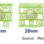
It is truly amazing to consider the advances in microelectronic process development, using 193i photolithography. The figure below is a stark reminder of the difference between the illuminating wavelength and the final imaged geometries. This technology evolution has been enabled by continued investment in mask data generation… Read More
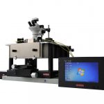
This year is shaping up to be an inflection point, when multi-die packaging technology will experience tremendous market growth. Advanced 2.5D/3D package offerings have been available for several years, utilizing a variety of technologies to serve as the package substrate, interposer material for embedding die micro-bump… Read More
At the Samsung theatre (cutely named the Samsung Open Collaboration (SoC) theater) I watched a presentation by KK Lin on using DFM to bring up their 14nm and 10nm processes. And yes, they are real. Here is a picture I took of a 14nm wafer and a 10nm wafer. Samsung announced that they would ramp 10n to volume production by the end of next… Read More
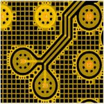
In modern electronic industry PCBs are required to accommodate highly dense circuits with large number of components and complex routing spaces. While the complexity is increasing, the time-to-market is decreasing. In such a scenario, there is no other option than to reduce the design time by employing innovative editing options… Read More
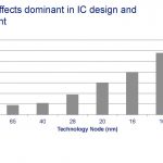
It’s less than four weeks to go at DAC 2015 and the program is final now. So I started investigating new technologies, trends, methodologies, and tools that will be unveiled and discussed in this DAC. In the hindsight of the semiconductor industry over the last year, I see 14nm technologies in the realization stage and 10nm beckoning… Read More
In last 30+ years, the electronic design industry has seen rapid changes more than any other industry. The change has taken place in the whole electronic ecosystem including semiconductor technology, transistor design, IC / SoC design, PCB, and system design. Today, a PCB can be very complex connecting several heterogeneous… Read More
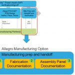
Getting a printed circuit board from design and into production presents one of the biggest challenges in successfully launching a product. The designer’s job is to anticipate issues that can adversely affect PCB fabrication and assembly. Design rules and component libraries go part of the way, but there is a thicket of things… Read More