Printed Circuit Boards (PCBs) are the foundation of modern electronics, and designing them efficiently is complex. Design automation and advanced PCB routing have transformed the process, making it faster and more reliable. Design automation streamlines tasks, reduces errors, and ensures consistency. Advanced PCB routing combines auto-routing and manual routing for efficiency, optimizes layer stacking, controls via placement, and handles differential pair routing.
Siemens EDA has published an eBook on PCB design automation covering problems with legacy PCB design methodologies, constraint-management in PCB design, PCB component placement and routing, design reuse and automating manufacturing output for PCB board fabrication. Following is an overview of the eBook.
Problems with Legacy PCB Design Methodologies
Legacy PCB design methodologies are struggling to meet the demands of modern electronics development. They are ill-suited for complex products, shorter timelines, reduced budgets, and limited resources. Manual data manipulation is error-prone and time-consuming, hindering integration between design tools. Communication bottlenecks between engineering and other disciplines, involving physical document exchange, no longer work in today’s fast-paced design environment. To keep up with evolving industry standards, more efficient and streamlined PCB design processes are essential.
Constraints-Management in PCB Design

Constraint management is a vital practice in PCB design, streamlining the process and reducing the need for extensive back-and-forth communication between engineers and designers. Constraint-driven methodology has become a best practice, allowing for the systematic management of constraints and introducing standardization. Constraint templates, which can be reused and adjusted for specific projects, save time and maximize existing data utilization.
This approach offers control over electrical and physical rules, aligning the design with the final product’s requirements. Design constraints ensure quality is integrated from the outset, eliminating the need for costly post-design quality checks. Automated constraint entry in Siemens EDA’s Xpedition simplifies the process and ensures adherence to predefined parameters, enhancing the potential for design success by consistently meeting specified requirements and constraints.
PCB Component Placement
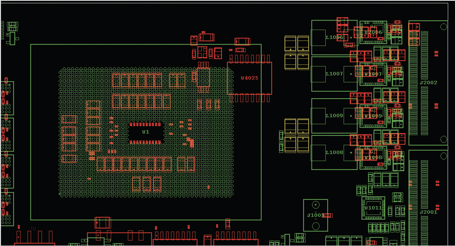
3D component planning and placement are pivotal in achieving a “correct-by-construction” PCB layout while considering electro-mechanical constraints. Clusters, defined groups of components within a circuit, play a crucial role in simplifying and optimizing placement. They enable efficient extraction, version control, and reuse of component groups, enhancing connectivity and flow. Clusters also support nested structures, allowing for unique rules within groups, streamlining component placement. In the Xpedition environment, clusters can be further enhanced with additional elements like mounting holes and seed vias, providing greater visibility and control over the PCB design process and improving design quality.
PCB Routing
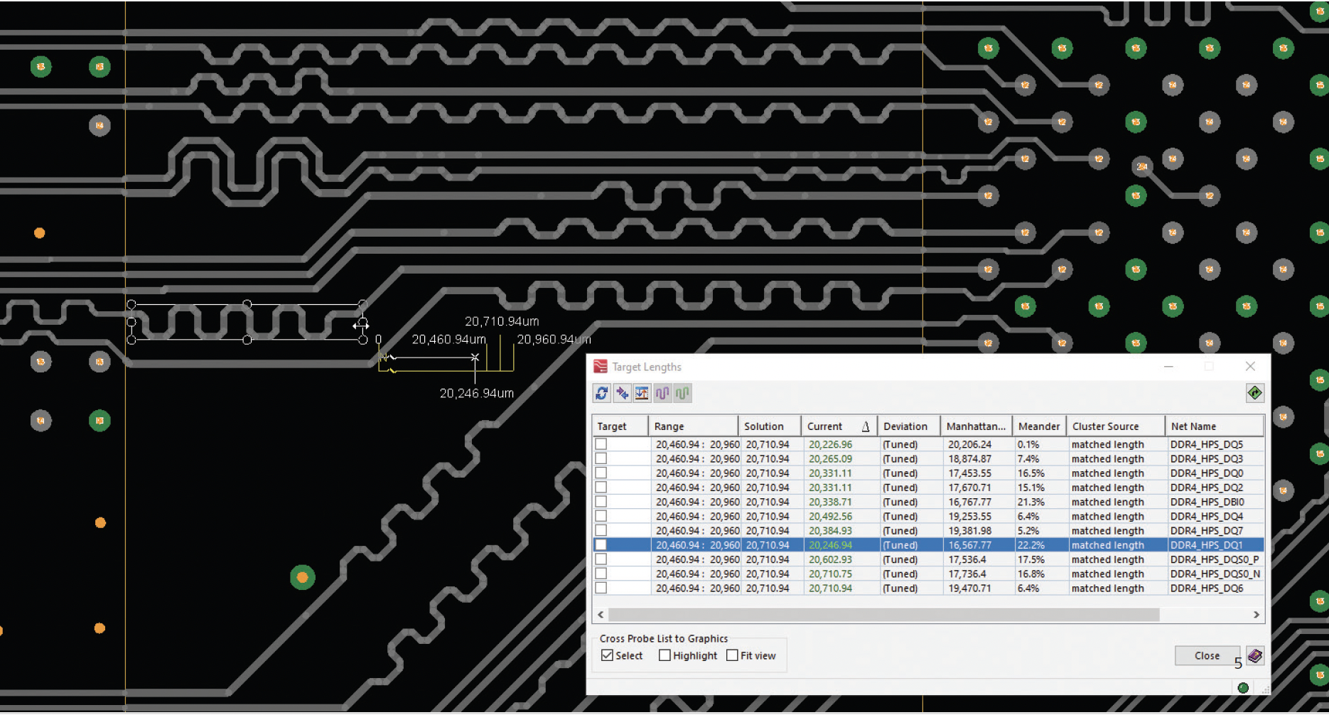
Modern PCB design tools offer various routing approaches, including manual, interactive, semi-automated, and fully automated methods, improving the design process’s efficiency. In the Xpedition flow, advanced routing features like Sketch Routing and Sketch Planning provide user-friendly automation for high-quality, fast routing. These tools mimic human decision-making, allowing designers to experiment with autorouting and modifications until they achieve the desired outcome, enhancing PCB routing efficiency.
Additionally, advanced routing tools like the “hug router” help manage stubborn nets without overhauling the design. It’s particularly useful for routing single net lines in pre-routed designs. The “plow routing” feature aids in handling challenging remaining nets, reducing time and effort. For specialized signal requirements in analog and RF traces, “hockey stick” or segment routing offers precise control over routing paths, improving routing precision and efficiency in PCB design.
Design Reuse in PCB design
Efficiency in PCB design can be greatly improved through the practice of PCB design reuse. This strategy involves leveraging previously approved circuitry or IP in various designs, saving time and reducing project risks. It eliminates redundant efforts, allowing the reuse of reliable components and layouts. True design reuse is more than traditional copy-pasting; it involves applying entire layouts, like multi-layer circuit stacks, saved in the library for future use, saving significant time compared to manual recreation. In platforms like Xpedition, creating and managing reuse modules is seamless, simplifying sharing and tracking deployment, making PCB design reuse an invaluable strategy in electronics design.

Automating Manufacturing Output for PCB Board Fabrication
Once a PCB design is fully complete and successfully passes various assessments, the focus turns to preparing for board fabrication and assembly manufacturing. Automation is key in this phase, eliminating redundancy and saving time in generating output files like ODB++, Gerber data, GENCAD data, and more. It ensures consistency in output generation, customizability to meet standards, and correctness and quality in the content. In contrast to manual methods, automation streamlines the process and provides a reliable foundation for successful printed circuit assembly production by fabricators and manufacturers.
Summary
In the world of PCBs, the cost of board respins due to human errors is significant in terms of both time and money. Early error detection is crucial, as errors discovered later become more expensive to rectify. Adopting a “correct-by-construction” design approach and leveraging automation tools such as Siemens EDA’s Xpedition Enterprise are very important.
To learn more, download the eBook guide for PCB Design Automation.
Getting educated on PCB design automation tools is also essential to avoid schedule disruptions due to a lack of knowledge on how to effectively use the tools. Siemens EDA offers training sessions, including on-demand training, expert-led webinars, and on-site visits with application engineers, to empower designers to harness the full potential of automation and streamline PCB design processes efficiently.
For more information on PCB design automation, visit:
https://eda.sw.siemens.com/en-US/pcb/engineering-productivity-and-efficiency/design-automation/
To request an on-site training, visit:
https://resources.sw.siemens.com/en-US/talk-to-an-expert-about-xpedition
Also Read:
Uniquely Understanding Challenges of Chip Design and Verification
Successful 3DIC design requires an integrated approach
Make Your RISC-V Product a Fruitful Endeavor
Share this post via:


Comments
There are no comments yet.
You must register or log in to view/post comments.