
Test is the Rodney Dangerfield of EDA, it doesn’t get any respect. All designs need to be tested but somehow synthesis, routing, analog layout and the rest are the sexy areas. In my spoof all purpose EDA keynote address I even dissed it:You are short on time so slip in a quick mention of manufacturing test. Who knows anything about it? But chips have to be tested so talk about scan. Or BIST. Or ScanBIST.
It is about a $120M business with Mentor being a little over half of it. But test is getting more important driven by two things. Firstly, chips are huge and consist of many IP blocks that were not designed and are barely understood by the SoC design team. Another big driver is 3D ICs (probably even more in the future). Testing a stack of die when only the lowest one is accessible to the tester creates its own set of challenges. But what is called the “known good die” problem is another driver. In a conventional (non 3D) IC, if a bad die makes it through to final test then a package needs to be discarded along with a die that was bad in any case. But in a 3D IC stack, if a bad die makes it all the way to final test, not only is the package and a bad die discarded, but several good die too. So wafer sort for 3D IC is much more important than before.

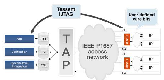
Mentor has just announced an IJTAG solution that addresses both these drivers, that chips increasingly consist of IP blocks which the designers do not fully understand and that 3D just adds another layer of complexity. It supports the catchily-named IEEE P1687 standard (IJTAG) and allows designers to easily reuse test, monitoring and debugging logic embedded in the IP blocks. It generates an integrated hierarchical contro9l and data network with a single top-level interface for the whole SoC. Any embedded instrumentation that is P1687 compliant can be used. It is especially valuable where pin count is limited or access is difficult (as in the 3D stacked die configurations).
The new IEEE P1687 standard creates an environment for plug-and-play integration of IP instrumentation, including control of boundary scan, built-in self-test (BIST), internal scan chains, and debug and monitoring features in IP blocks. The standard defines hardware rules related to instrumentation interfaces and connectivity between these interfaces, a language to describe these interfaces and connectivity, and a language to define operations to be applied to individual IP blocks. IJTAG replaces proprietary and incompatible IP interfaces from multiple suppliers with a standardized interface mechanism that enables plug-and-play integration of IP test and instrumentation facilities.
Mentor’s Tessent IJTAG solution provides automated support for the IJTAG standard, substantially reducing the time and effort required to assemble large SoC designs from reusable IP blocks. The new product includes all the facilities needed to efficiently integrate IEEE P1687-compliant IP into a design:
- Automatic verification that a given IP block is compliant to the P1687 standard
- Verification that P1687-compliant IP blocks are properly connected within a P1687-compliant access network
- Automatic creation of a P1687-compliant access network connecting IP to the top level instrument interface
- Retargeting and merging of local IP instrumentation patterns through the P1687 network, allowing IP specific sequences to be applied from chip pins or from anywhere higher up in the system hierarchy
The white paper on Tessent IJTAG is here.


Comments
There are no comments yet.
You must register or log in to view/post comments.