
I was invited to give a talk at the ISS conference on the Impact of EUV on the Semiconductor Supply Chain. The ISS conference is an annual gathering of semiconductor executives to review technology and global trends. In this article I will walk through my presentation and conclusions.
Why EUV
Companies used to talk about implementing EUV when it was less expensive than optical, however other factors are now driving the adoption of EUV:
[LIST=1]
Who Needs EUV?
- NAND – NO – with the 2D to 3D transition well underway (3D bit production crossed over 2D bit production in 2017), NAND has transitioned from lithography scaling to layer scaling. 3D NAND has relatively large lithographic features and is driven more by deposition and etch.
- Logic – YES – 7nm is ramping now with mid-80s mask counts for optical processes. 5nm logic will have >100 masks and cycle times of up to 6 months. We expect EUV to be implemented for second and third generation 7nm logic processes.
- DRAM – YES but delayed relative to logic. DRAM has simpler processes with roughly one half the masks of a 5nm logic process and fewer multi-patterning masks. Samsung has already ramped 1x DRAM (18nm) and is ramping 1y DRAM both without EUV. We expect EUV to be implemented for DRAM, but logic will go first.
First Generation 7nm Foundry Logic (7)
TSMC released their 7FF process to production in Q3 of 2017 and is ramping it up now. GLOBALFOUNDRIES (GF) is expected to ramp their 7LP process later this year. Both processes are optical based with no EUV layers. The minimum metal pitch (MMP) for both process is 40nm produced with SADP resulting in a 1D metal pattern.
Second Generation 7nm Foundry Logic (7c)
At their technology symposium last year GF discussed their first step into EUV as using EUV for contacts and vias at 7nm without a pellicle. Contacts and vias have low open area (around a few %) so that particles landing on the reticle are unlikely to result in a printed defect. Producing contacts and vias without a pellicle maximizes throughput and eliminates the need for a pellicle as a requirement to start using EUV. There isn’t enough data available yet to be certain this will result in acceptable yield but it is believed it will. TSMC has not publicly announced a similar plan but they are reportedly discussing it privately. 7c is relatively easy to implement, it doesn’t result in a shrink, but no redesign is needed and 7c improves cycle time by replacing 15 optical layers with 5 EUV layers, EPE and electrical distributions are also improved.
In order to implement 7c we need the following:
- A high throughput EUV tool – the exact power and throughput is somewhat in flux, ASML has multiple knobs to tune throughput and they are trying to maximize throughput and uptime. With NXE3400b systems shipping now this requirement should be met.
- >90% uptime – at IEDM in December Intel said their EUV uptime was only around 75%. In my interviews with lithographers while building this presentation this was major issue. ASML has uptime improvement plans and the NXE3400b is expected to be better, ASML needs to execute on this.
- Pellicle – if a pellicle is necessary then a pellicle that can survive the source power being used will be needed. This should be available.
- Reticle inspection – eBeam inspection can be used although not optimal.
- Photoresists – current photoresists are good enough for 7nm although dose may be higher than desired at 30mJ/cm[SUP]2[/SUP] versus a 20mJ/cm[SUP]2[/SUP] target.
I expect to see 7c in production in early 2019.
Third Generation 7nm Foundry Logic (7+)
TSMC and GF have both announced 7nm + plans that add 1x metal layers to contact and vias for EUV. This would result in a shrink and require TSMC and GF customers to do a redesign. This will also be where Samsung’s 7LPP process comes in because it will have EUV for metal. In order to use EUV for metal a pellicle is required because metal has high open area. I expect the MMP to be 36nm and by using EUV the design can be a 2D pattern instead of 1D used at 7 and 7c. This means that not only will the pitch decrease from 40nm to 36nm shrinking designs but moving from 1D to 2D will improve routing and provide additional shrink. 7+ will replace 23 optical layers with 9 EUV layers.
In order to implement 7+ we need the following:
- The same items as 7c.
- Redesigns for TSMC and GF, 7 and 7c products.
- A pellicle and ideally one with >90% transmission.
- Actinic inspection is desirable, but the pellicle can be removed for eBeam inspection and then reattached.
I expect 7+ to ramp in mid to late 2019.
What About Intel
Intel 10nm is ramping now and is similar to foundry 7+ processes. Intel 10nm does have some scaling boosters the foundries haven’t used and may be denser for random logic, but the foundries have smaller SRAM cell size the denser process will be design dependent.
During a recent interview with Intel’s director of lithography Janice Golda she indicated Intel has not decided on a node for EUV introduction but will introduce it when ready.
Intel process introductions stretching out, when will 7nm ramp? Intel has said 2020 but that could slip.
Intel plans a 10+ and 10++ process and when asked if Intel might introduce EUV for one of these processes if it is ready Janice said they could. For planning purposes I am assuming 10+ for EUV introduction in 2019.
5nm Foundry Logic (5)
More extensive EUV use for 11 or 12 layers. EUV for contacts and vias and critical metal layers, possibly EUV for fin cuts.
Fins and gates are currently produced with SAQP and SADP respectively. Because SADP and SAQP make smooth lines and spaces that are desirable for transistor formation, I expect SADP and SAQP to continue to be used even after EUV is introduced. However, at 5nm fin formation will require 4 or 5 cut masks with SAQP and this could be replaced with a single EUV cut mask.
MMP will be 26nm, the 1D EUV pitch limit.
Samsung’s roadmap calls for 6nm and 5nm in 2019 and TSMC has also announced 5nm in 2019. GF has not announced a 5nm introduction date and I have assumed 2020 for planning purposes.
In order to implement 5 we need the following:
- The same items at 7c/7+
- Pellicle must be 90% or better transmission.
- Actinic inspection is highly desirable.
- Much better photoresist. One lithographer said that defectivity is an order of magnitude too high for 5nm and also that doses would likely be around 70mJ/cm[SUP]2[/SUP]. Doses go up as pitch is shrunk unless the photoresist is improved, and we need <50mJ/cm[SUP]2[/SUP] for reasonable throughput. With 6nm/5nm expected in late 2019 this only leaves 12 to 18 months to improve the photoresist.
EUV Throughput
It is important to understand how pellicle throughput and dose impact throughput. ASML has a number of tuning knobs they can use to optimize EUV tools and I don’t have access to their throughput models. The following is a simplistic approximation of throughput. The throughputs illustrated here aren’t absolute but give an indication of the relative impact.
The first thing to understand is the light path through the exposure tool. The EUV light goes through the pellicle (if used), bounces off the reticle, and then goes back through the pellicle (if used). There is also an optional membrane that is “pellicle like” although with higher transmission. Figure 1 illustrates the light path.
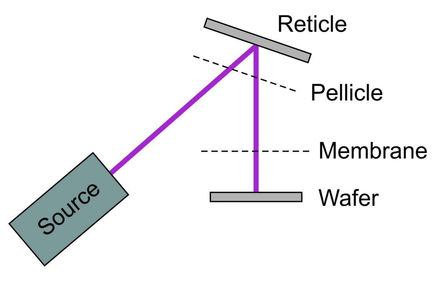
Figure 1. Exposure tool light path.
Pellicles currently have 83% transmission resulting in 69% of the light reaching the wafer with a pellicle and ~60% if a membrane is also used. If the pellicle transmission is improved to 90%, then 81% of the light reaches the wafer for a pellicle only and 77% of the light reaches the wafer with a pellicle and membrane.
Figure 2 shows throughput versus dose and transmission.
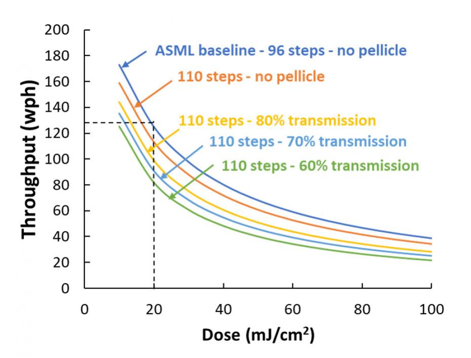
Figure 2. EUV system throughput.
The dotted lines on figure 2 represent 125wph previously announced by ASML for a 250-watt source, 96 steps, no pellicle and a 20mJ/cm[SUP]2[/SUP] dose. At ISS ASML talked about getting 125wph at a lower source power allowing them to run the source at lower power for higher uptime. The throughput goes down if more steps are required to cover the wafers and the average steps for logic is around 110. Logic die don’t fill the entire reticle field requiring some overlap. Figure 2 illustrates the strong effect on throughput that dose has. ASML has options to flatten out these curves but dose is still a key throughput factor.
Dose and Throughput
From figure 2 we can see that increasing dose reduces throughput. Based on my discussions with multiple lithographers working with EUV tools the current expectation at 7nm is a 30mj/cm[SUP]2[/SUP] dose. At 5nm the dose is expected to rise to 70mJ/cm[SUP]2[/SUP] unless there is significant improvement in the photoresist. A dose of <50mJ/cm[SUP]2[/SUP] is needed to provide reasonable throughput. Once again only 12 to 18 months remain to complete this work in time for planned 6nm/5nm introductions.
Wafer Volume Forecast
After projecting the ramp up of 7 (&i10), 7c, 7+ (and i10+) by year and company I have developed the wafer volume forecast shown in figure 3 (in thousands of wafers per year).
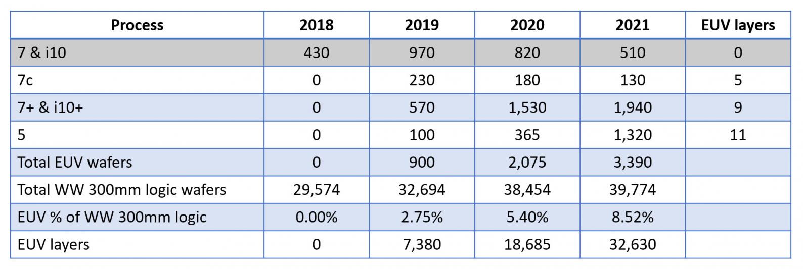
Figure 3. Wafer Volumes (thousands).
This is a logic wafer forecast, additional DRAM wafers are expected in 2020 and 2021. Worldwide 300mm logic wafer capacity is included in the chart and the percentage of these wafers that will be produced with EUV is calculated. The calculated percentages are 2.75%, 5.40% and 8.52% in 2019, 2020 and 2021 respectively. Worldwide 300mm logic wafer capacity is from the IC Knowledge – 300mm Watch database – 2017 – revision 06.
The number of EUV layers this represents is also provided. I have compared the number of layers required to the number of EUV tools expected to be on-line by year and after accounting for conservative throughput projections this will consume most of the available capacity with some left over for DRAM. I have shown these layers projection to ASML and they are reasonably aligned with ASML’s expectations.
Masks
Figure 4 presents projected mask counts and resulting cycle time for 7, 7c, 7+ and 5. The key take away from this graph is that a 5nm optical solution would have an approximately 6 month cycle time and 5nm with EUV will be <4 months.
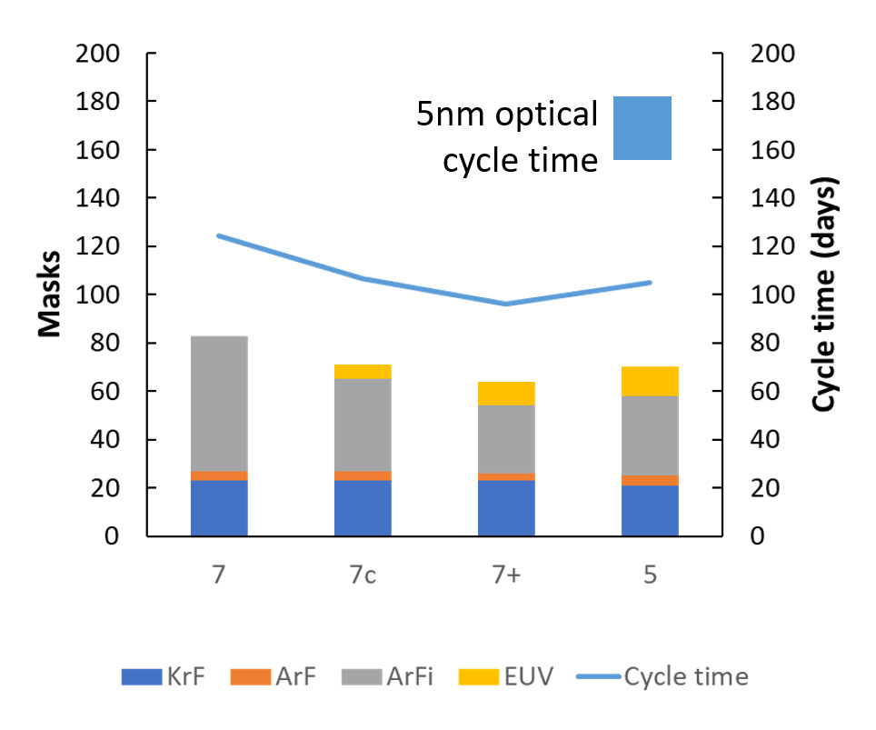
Figure 4. Mask counts and cycle time versus process variant.
Cost
In figure 5 I have compared forecast wafer and capital cost, cleanroom area and cycle time for 7c versus 7. I have assumed a 40k wpm greenfield fab in Taiwan that is still depreciating. Currently 7nm EUV masks are approximately 6x the cost of ArFi mask and although this is expected to come down as production ramps up I have assumed this as a conservation assumption. The 7 process is 83 optical masks and the 7c process is 68 optical masks and 5 EUV masks. I have assumed a 250 watts source at 90% uptime without a pellicle and a 30mJ/cm[SUP]2[/SUP] dose. Throughputs are per figure 2 and the calculations were done using the IC Knowledge – Strategic Cost Model – 2017 – revision 5.
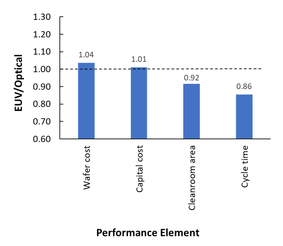
Figure 5. Relative EUV costs and performance versus optical at 7nm.
From figure 5 we can see that costs are similar, but cleanroom size and cycle time are better. EPE and electric distributions would also be better but are not shown.
Reticle Amortization
As I mentioned previously, EUV reticle costs are currently approximately 6x ArFi reticle costs. Mike Lercel of ASML worked with Photronics to estimate mature EUV reticle costs once production volumes are reached. The conclusion was 2x to 3x, numbers that seem reasonable to me.
In figure 6 I show the amortization costs for a complete reticle set for 5nm comparing optical to a set with EUV reticles at 6x, 4x, and 2x the cost of ArFi reticle costs. The two reticle set costs are similar when EUV is 4x the cost of ArFi because most of the multi-patterning replaced by EUV uses 4 ArFi masks. At <4x cost that should be achievable, EUV reticle set costs will be cheaper than optical reticle sets.
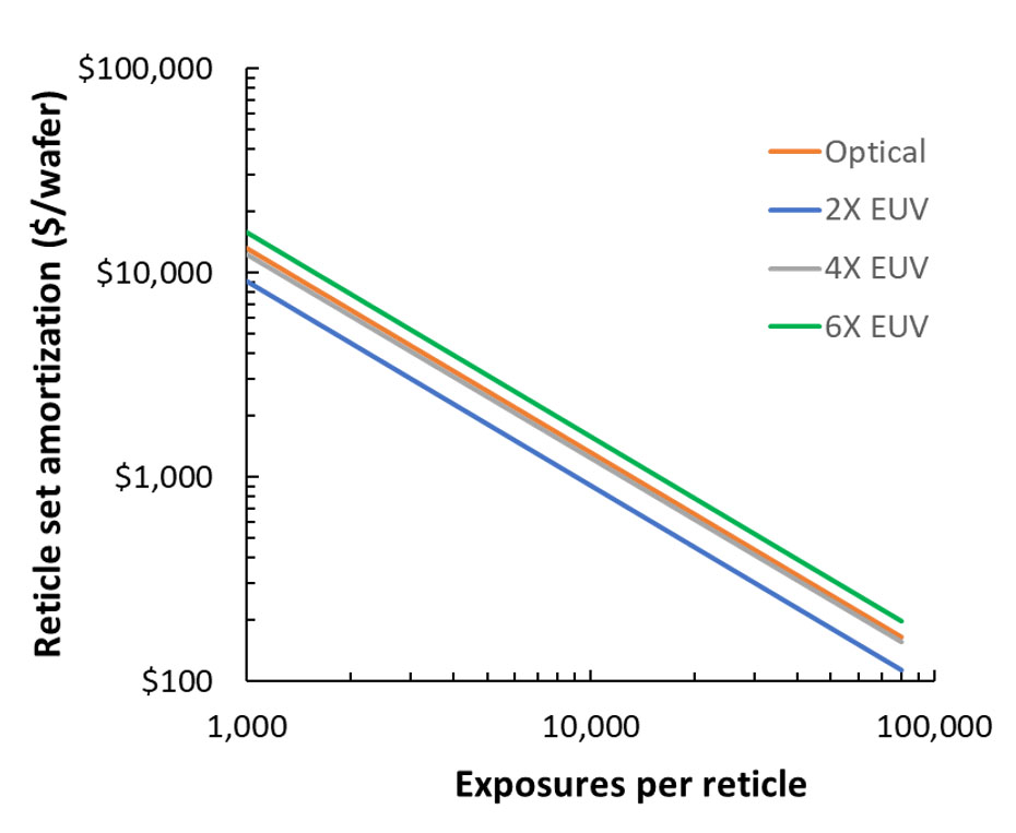
Figure 6. Reticle set amortization.
Another key take away is that for optical or EUV reticle sets at 5nm, high volumes of wafers have to be run on the reticle set for the reticle amortization to be affordable. This is part of a bigger industry problem where design costs and reticle set costs are so high for leading edge technologies that only the highest volume products can affordably utilize the processes.
Logic Process Steps
In order to gage the impact of EUV on the equipment industry, figure 7 plots ALD/CVD depositions, dry etch/ash and exposure steps for 7, 7c, 7+ and 5. There is some decline in ALD/CVD steps as EUV is implemented but most of the loss is recovered at 5 due to higher process complexity. There is more loss for dry etch/ash and less recovery at 5.
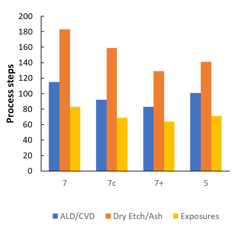
Figure 7. Process steps by type.
With EUV representing less than 10% of logic wafers even in 2021 and the relatively small declines in deposition and etch/ash steps going from 7 to 5 we don’t see EUV having much impact on the equipment industry. It should also be noted that 3D NAND is ramping rapidly and 3D NAND uses a relatively large number of deposition and etch tools.
Logic Material Spending
Like the process steps and equipment impacts, figure 8 illustrates the effect on material spending and once again I don’t expect much impact except perhaps in a few isolated sub segments.
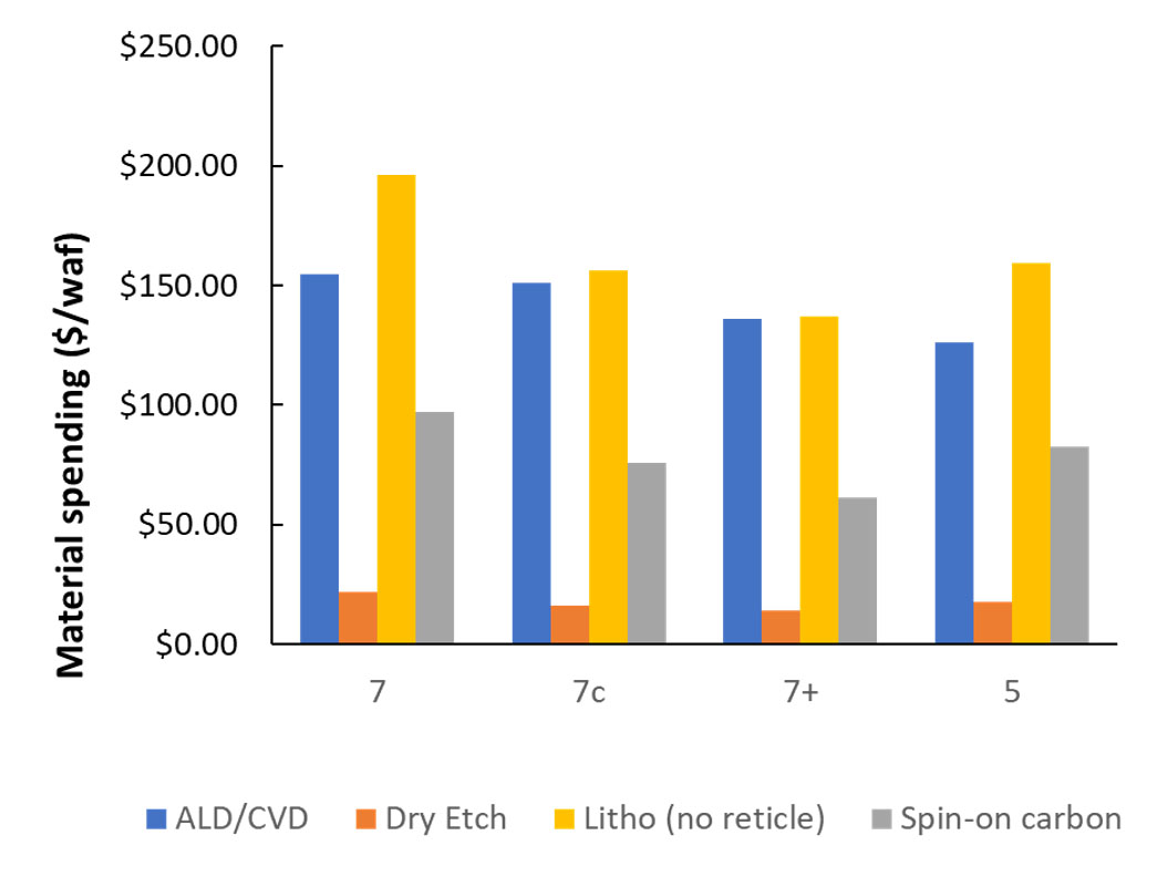
Figure 8. Material spending by type.
Conclusion
At the completion of this analysis I have come to four main conclusions:
[LIST=1]
Thank You
I held many useful discussions with lithography experts while putting this presentation together, some declined to be named but have my gratitude for their help. The following experts gave me permission to list them and I want to publicly thank them: Mike Lercel of ASML, Harry Levinson of Global Foundries, and Janice Golda of Intel.
Full presentation is HERE.
Share this post via:


Comments
17 Replies to “ISS 2018 – The Impact of EUV on the Semiconductor Supply Chain”
You must register or log in to view/post comments.