Curvilinear Design Primer for Design, Packaging Communities
This interview was done by Bob Smith, Executive Director, ESD Alliance, a SEMI Technology Community.
Previously, Fujimura served as CTO at Cadence Design Systems and returned to Cadence for the second time through the acquisition of Simplex Solutions where he was President/COO and inside board member. He was also an inside board member and VP at Pure Software. Simplex and Pure both went public during his tenure. Fujimura was a founding member of Tangent Systems, subsequently acquired by Cadence Design Systems. He was a board member of HLDS, RTime, Bristol, S7, and Coverity, Inc., all of which were successfully acquired. Fujimura received Bachelor of Science and Master of Science degrees in Electrical Engineering from MIT.
Semiconductor packaging and photomask segments of our industry have undergone some major technology changes in the past few years after relatively minor changes for many years. In the case of photomasks, new technologies such as multi-beam mask writers and extreme ultraviolet (EUV) lithography are major breakthroughs in the news as they ramp into high-volume manufacturing. A new trend related to these technologies is the use of curvilinear features on photomasks.
Curvilinear photomasks are here today, particularly interesting to the ESD Alliance as the door opens for “curvy” design. Aki Fujimura, CEO of D2S and a member of the the ESD Alliance Governing Council, speaks to me about curvilinear photomasks and what it means for design and packaging.
BS: What are the advantages of curvilinear photomasks?
AF: First let me explain what we mean by curvilinear photomasks. Shapes consisting of axis-parallel edges are sometimes referred to as Manhattan geometries. Shapes that do not need to be Manhattan geometries are considered curvilinear in the context of our discussion.
Curvilinear mask features have been shown not only to print more accurately, mostly because 90-degree corners can’t be accurately reproduced, but also to print more reliably, with less variation. This is good for both mask and wafer quality.
BS: What breakthroughs enabled curvilinear photomasks?
AF: Multi-beam mask writing and GPU-acceleration of pixel-based computing including curvilinear inverse lithography technology (ILT) are enabling curvilinear masks. With multi-beam mask writers available in all leading-edge mask shops now, the mask write times are no longer affected by the number of shapes on the mask or their complexity. This is principally because multi-beam mask writers write with pixels, similarly to how TVs, monitors, and digital projection machines work.
The economics of mask writing is dominated by the mask writing time. The fact that multi-beam mask writers, given a resist and writing method, writes any shapes of any shape count in constant time is economically and logistically very attractive to the mask shop. Once a mask shop has a multi-beam mask writer, curvilinear masks take no more time to write than any other.
BS: What is ILT and how does it contribute?
AK: ILT is a mathematically rigorous inverse version of optical proximity correction (OPC) known to produce the best wafer results for both optical (193i) and EUV lithography. Many studies have demonstrated that curvilinear ILT mask shapes produce the best “process windows,” a measure of resilience to manufacturing variation.
Until multi-beam mask writers became available in the leading-edge mask shops, it hadn’t been practically possible to use curvilinear mask shapes as the desired mask shapes provided to the mask writers. However, runtimes associated with this computational technique limited its practical application to critical “hotspots” on chips.
Applying GPU acceleration to the ILT problem paved the way in the past few years for some breakthroughs in runtime roadblocks to ILT. In 2019, an entirely new approach systematically designed for multi-beam mask writers and GPU acceleration by D2S made full-chip ILT a practical reality in production for the first time.
BS: Will curvilinear masks be used for 193i lithography, EUV or both?
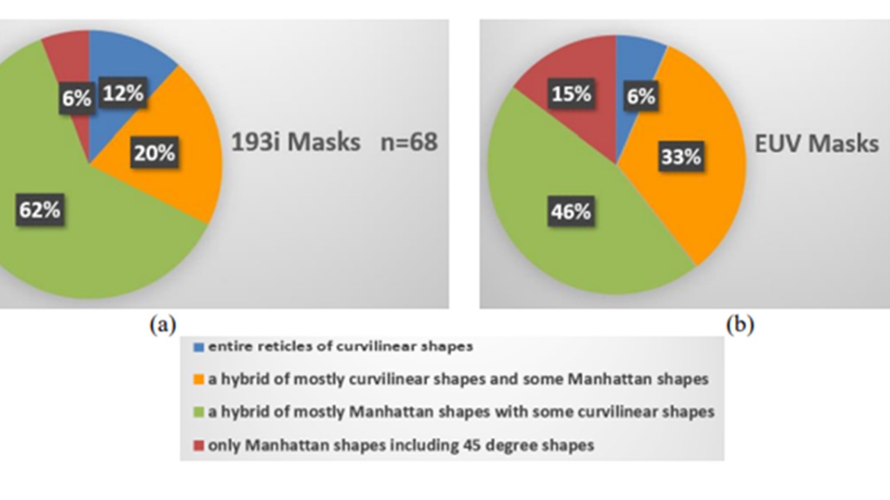
AF: In annual surveys conducted by the eBeam Initiative (See Figure 1), industry experts anticipate that curvilinear ILT shapes are already in use or will be for hotspots in some leading-edge layers before 2023 for both 193i and EUV masks. They clearly indicate that the primary reason to purchase multi-beam mask writers is for EUV masks. They also indicate that writing curvilinear masks is also a strong reason to purchase multi-beam mask writers.
Given that EUV masks are being written with multi-beam mask writers already, there is no penalty in the mask write time to write curvilinear shapes. Whether for 193i or for EUV, curvilinear mask shapes produce better wafer quality. With sufficient supply of multi-beam writers, leading-edge masks are likely to be written with them in the future.

Figure 1 caption: 2020 eBeam Initiative Survey result in answer to the question: “How extensively will curvilinear shapes be used for leading-edge (EUV, 193i) masks intended for high-volume manufacturing (HVM) by 2023?” (a) 94% believe curvilinear shapes will be used for 193i for HVM by 2023, (b) 85% expect that EUV also needs curvilinear shapes for HVM.
Source: eBeam Initiative
BS: Where is the industry in terms of adoption of curvilinear photomasks?
AF: With multi-beam mask writing being widely available for the leading-edge nodes, manufacturing curvilinear ILT shapes is now possible.
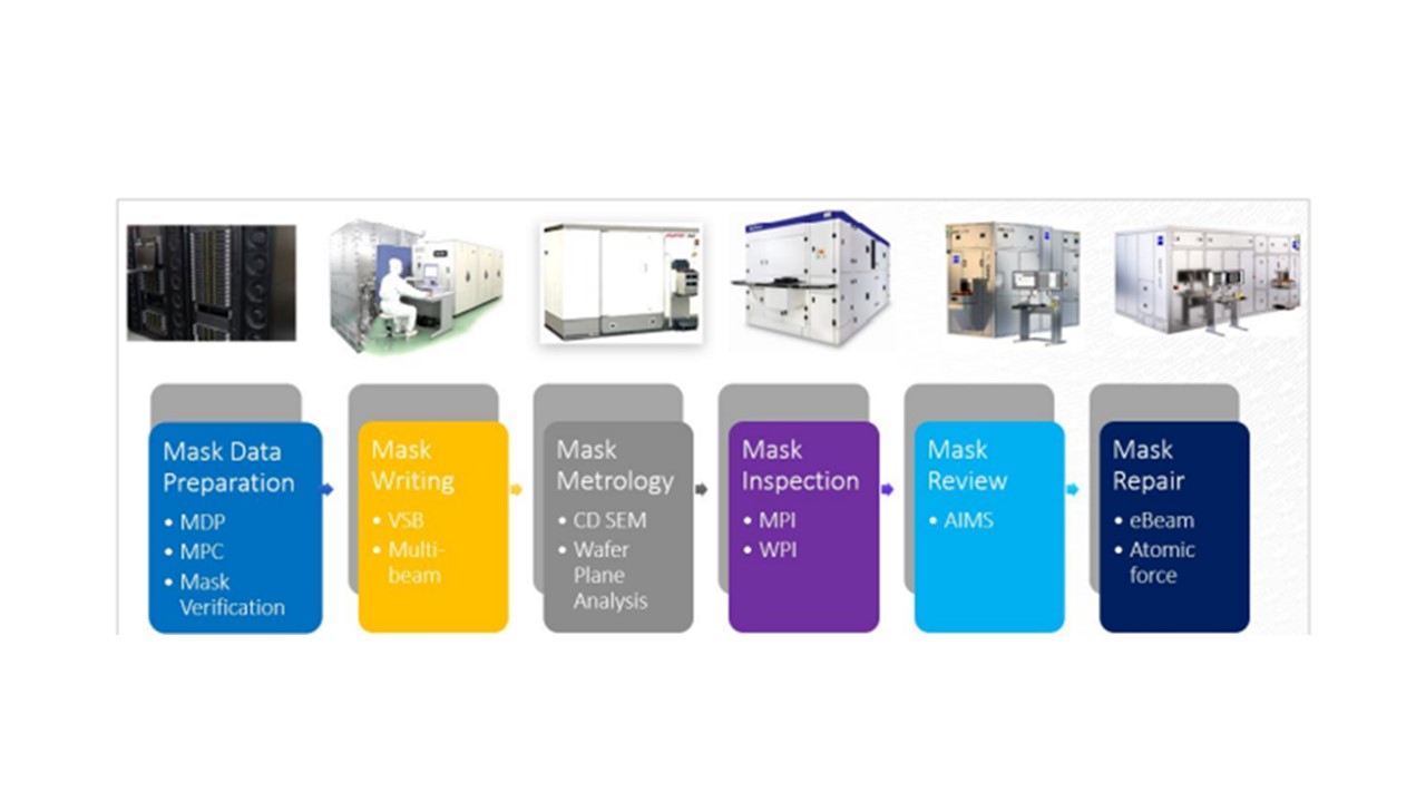
And the rest of the mask making infrastructure shown in Figure 2? A limited number of curvilinear shapes can already be handled by leading-edge mask shops today, according to leading authorities. For wide-spread use, there are likely more streamlined solutions needed for metrology, inspection, dispositioning and repair.

Figure 2 caption: A typical photomask manufacturing flow follows a specific pattern.
Source: D2S
BS: How do curvilinear photomasks unlock new opportunities for design?
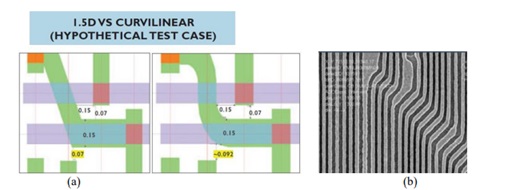
AF: As we anticipate this exciting transition to curvilinear mask making or “curvy” design, an upstream effect of this change is being studied by some. Figure 3(a) below shows an image from an Imec paper in 2019 that highlighted potential improvements in compacting cell designs, decreasing load, and decreasing interconnect delay through the use of curvy design. Figure 3(b) from a Micron presentation illustrates the use of manual manipulation to jog multi-bit busses using non-Manhattan, curvilinear shapes of varying angles. Manual manipulation is resource intensive, a clear indication of the benefits being significant enough to be worth the trouble, at least for a memory maker. The entire chip design infrastructure is based on the Manhattan assumption.
In my previous life in EDA, I had something to do with that, so I know this very well and it is not going to change any time soon. At the same time, though, is there any doubt that a curvilinear chip, if magically made possible, would be smaller, faster, and use less power?

Figure 3 caption: (a) An Imec paper showing “curvy” designs are feasible with the reliable manufacturing of curvy masks, (b) an example wafer image from Micron with non-Manhattan design.
Source: D2S
Also Read
CEO Interview: Frankwell Lin, Chairman and CEO of Andes Technology
CEO Interview: Tamas Olaszi of Jade Design Automation
CEO Interview: John Mortensen of Comcores
Share this post via:


Comments
There are no comments yet.
You must register or log in to view/post comments.