Threads
XF\Mvc\Entity\ArrayCollection Object
(
[entities:protected] => Array
(
[25489] => ThemeHouse\XPress\XF\Entity\Thread Object
(
[_uniqueEntityId:XF\Mvc\Entity\Entity:private] => 57
[rootClass:protected] => XF\Entity\Thread
[_useReplaceInto:protected] =>
[_newValues:protected] => Array
(
)
[_values:protected] => Array
(
[thread_id] => 25489
[node_id] => 2
[title] => Japan’s Rapidus Takes on TSMC With Aggressive 2nm Pricing
[reply_count] => 5
[view_count] => 822
[user_id] => 5
[username] => Daniel Nenni
[post_date] => 1783708942
[sticky] => 0
[discussion_state] => visible
[discussion_open] => 1
[discussion_type] => discussion
[first_post_id] => 101605
[first_post_reaction_score] => 0
[first_post_reactions] => []
[last_post_date] => 1783838879
[last_post_id] => 101633
[last_post_user_id] => 20231
[last_post_username] => Barnsley
[prefix_id] => 0
[tags] => []
[custom_fields] => []
[vote_score] => 0
[vote_count] => 0
[featured] => 0
[type_data] => []
[index_state] => default
)
[_relations:protected] => Array
(
[User] => ThemeHouse\XLink\XF\Entity\User Object
(
[_uniqueEntityId:XF\Mvc\Entity\Entity:private] => 54
[rootClass:protected] => XF\Entity\User
[_useReplaceInto:protected] =>
[_newValues:protected] => Array
(
)
[_values:protected] => Array
(
[user_id] => 5
[username] => Daniel Nenni
[username_date] => 0
[username_date_visible] => 0
[email] => dnenni@semiwiki.com
[custom_title] => Founder
[language_id] => 1
[style_id] => 0
[style_variation] =>
[timezone] => America/Los_Angeles
[visible] => 1
[activity_visible] => 1
[user_group_id] => 3
[secondary_group_ids] => 4,5,132
[display_style_group_id] => 3
[permission_combination_id] => 88
[message_count] => 15798
[question_solution_count] => 0
[conversations_unread] => 0
[register_date] => 1280720820
[last_activity] => 1783834816
[last_summary_email_date] => 1605968657
[trophy_points] => 113
[alerts_unviewed] => 111
[alerts_unread] => 111
[avatar_date] => 1663211649
[avatar_width] => 110
[avatar_height] => 107
[avatar_highdpi] => 0
[avatar_optimized] => 0
[gravatar] =>
[user_state] => valid
[security_lock] =>
[is_moderator] => 1
[is_admin] => 1
[is_banned] => 0
[reaction_score] => 9656
[warning_points] => 0
[is_staff] => 1
[secret_key] => 0HwyUVVHCwJotUUVEpvqAclfYJdGNPpw
[privacy_policy_accepted] => 0
[terms_accepted] => 0
[vote_score] => 0
)
[_relations:protected] => Array
(
)
[_previousValues:protected] => Array
(
)
[_options:protected] => Array
(
)
[_deleted:protected] =>
[_readOnly:protected] =>
[_writePending:protected] =>
[_writeRunning:protected] =>
[_errors:protected] => Array
(
)
[_whenSaveable:protected] => Array
(
)
[_cascadeSave:protected] => Array
(
)
[_behaviors:protected] =>
)
[Forum] => XF\Entity\Forum Object
(
[_uniqueEntityId:XF\Mvc\Entity\Entity:private] => 56
[rootClass:protected] => XF\Entity\Forum
[_useReplaceInto:protected] =>
[_newValues:protected] => Array
(
)
[_values:protected] => Array
(
[node_id] => 2
[discussion_count] => 8853
[message_count] => 64592
[last_post_id] => 101633
[last_post_date] => 1783838879
[last_post_user_id] => 20231
[last_post_username] => Barnsley
[last_thread_id] => 25489
[last_thread_title] => Japan’s Rapidus Takes on TSMC With Aggressive 2nm Pricing
[last_thread_prefix_id] => 0
[moderate_threads] => 0
[moderate_replies] => 0
[allow_posting] => 1
[count_messages] => 1
[auto_feature] => 0
[find_new] => 1
[allow_index] => allow
[index_criteria] =>
[field_cache] => []
[prefix_cache] => []
[prompt_cache] => []
[default_prefix_id] => 0
[default_sort_order] => last_post_date
[default_sort_direction] => desc
[list_date_limit_days] => 0
[require_prefix] => 0
[allowed_watch_notifications] => all
[min_tags] => 0
[forum_type_id] => discussion
[type_config] => {"allowed_thread_types":["poll"]}
)
[_relations:protected] => Array
(
[Node] => XF\Entity\Node Object
(
[_uniqueEntityId:XF\Mvc\Entity\Entity:private] => 55
[rootClass:protected] => XF\Entity\Node
[_useReplaceInto:protected] =>
[_newValues:protected] => Array
(
)
[_values:protected] => Array
(
[node_id] => 2
[title] => SemiWiki Main Forum ( Ask the Experts! )
[description] => Post your questions to the experts here!
[node_name] =>
[node_type_id] => Forum
[parent_node_id] => 1
[display_order] => 1
[display_in_list] => 1
[lft] => 2
[rgt] => 3
[depth] => 1
[style_id] => 0
[effective_style_id] => 0
[breadcrumb_data] => {"1":{"node_id":1,"title":"Main Category","depth":0,"lft":1,"node_name":null,"node_type_id":"Category","display_in_list":true}}
[navigation_id] =>
[effective_navigation_id] =>
)
[_relations:protected] => Array
(
)
[_previousValues:protected] => Array
(
)
[_options:protected] => Array
(
)
[_deleted:protected] =>
[_readOnly:protected] =>
[_writePending:protected] =>
[_writeRunning:protected] =>
[_errors:protected] => Array
(
)
[_whenSaveable:protected] => Array
(
)
[_cascadeSave:protected] => Array
(
)
[_behaviors:protected] =>
)
)
[_previousValues:protected] => Array
(
)
[_options:protected] => Array
(
)
[_deleted:protected] =>
[_readOnly:protected] =>
[_writePending:protected] =>
[_writeRunning:protected] =>
[_errors:protected] => Array
(
)
[_whenSaveable:protected] => Array
(
)
[_cascadeSave:protected] => Array
(
)
[_behaviors:protected] =>
)
[25494] => ThemeHouse\XPress\XF\Entity\Thread Object
(
[_uniqueEntityId:XF\Mvc\Entity\Entity:private] => 61
[rootClass:protected] => XF\Entity\Thread
[_useReplaceInto:protected] =>
[_newValues:protected] => Array
(
)
[_values:protected] => Array
(
[thread_id] => 25494
[node_id] => 2
[title] => Nvidia, CoreWeave, and Nebius: Inside the Circular Financing of the GPU Boom
[reply_count] => 1
[view_count] => 120
[user_id] => 36640
[username] => soAsian
[post_date] => 1783836819
[sticky] => 0
[discussion_state] => visible
[discussion_open] => 1
[discussion_type] => discussion
[first_post_id] => 101631
[first_post_reaction_score] => 1
[first_post_reactions] => {"3":1}
[last_post_date] => 1783838742
[last_post_id] => 101632
[last_post_user_id] => 20231
[last_post_username] => Barnsley
[prefix_id] => 0
[tags] => []
[custom_fields] => []
[vote_score] => 0
[vote_count] => 0
[featured] => 0
[type_data] => []
[index_state] => default
)
[_relations:protected] => Array
(
[User] => ThemeHouse\XLink\XF\Entity\User Object
(
[_uniqueEntityId:XF\Mvc\Entity\Entity:private] => 58
[rootClass:protected] => XF\Entity\User
[_useReplaceInto:protected] =>
[_newValues:protected] => Array
(
)
[_values:protected] => Array
(
[user_id] => 36640
[username] => soAsian
[username_date] => 0
[username_date_visible] => 0
[email] => jackmtsai@gmail.com
[custom_title] =>
[language_id] => 1
[style_id] => 0
[style_variation] =>
[timezone] => America/Chicago
[visible] => 1
[activity_visible] => 1
[user_group_id] => 2
[secondary_group_ids] =>
[display_style_group_id] => 2
[permission_combination_id] => 8
[message_count] => 447
[question_solution_count] => 0
[conversations_unread] => 0
[register_date] => 1608139716
[last_activity] => 1783836827
[last_summary_email_date] => 1719670845
[trophy_points] => 63
[alerts_unviewed] => 2
[alerts_unread] => 2
[avatar_date] => 0
[avatar_width] => 0
[avatar_height] => 0
[avatar_highdpi] => 0
[avatar_optimized] => 0
[gravatar] =>
[user_state] => valid
[security_lock] =>
[is_moderator] => 0
[is_admin] => 0
[is_banned] => 0
[reaction_score] => 406
[warning_points] => 0
[is_staff] => 0
[secret_key] => 2oKeCTFkGUpMro5tcmj7WaY9HksB13Kw
[privacy_policy_accepted] => 1608139716
[terms_accepted] => 1608139716
[vote_score] => 0
)
[_relations:protected] => Array
(
)
[_previousValues:protected] => Array
(
)
[_options:protected] => Array
(
)
[_deleted:protected] =>
[_readOnly:protected] =>
[_writePending:protected] =>
[_writeRunning:protected] =>
[_errors:protected] => Array
(
)
[_whenSaveable:protected] => Array
(
)
[_cascadeSave:protected] => Array
(
)
[_behaviors:protected] =>
)
[Forum] => XF\Entity\Forum Object
(
[_uniqueEntityId:XF\Mvc\Entity\Entity:private] => 56
[rootClass:protected] => XF\Entity\Forum
[_useReplaceInto:protected] =>
[_newValues:protected] => Array
(
)
[_values:protected] => Array
(
[node_id] => 2
[discussion_count] => 8853
[message_count] => 64592
[last_post_id] => 101633
[last_post_date] => 1783838879
[last_post_user_id] => 20231
[last_post_username] => Barnsley
[last_thread_id] => 25489
[last_thread_title] => Japan’s Rapidus Takes on TSMC With Aggressive 2nm Pricing
[last_thread_prefix_id] => 0
[moderate_threads] => 0
[moderate_replies] => 0
[allow_posting] => 1
[count_messages] => 1
[auto_feature] => 0
[find_new] => 1
[allow_index] => allow
[index_criteria] =>
[field_cache] => []
[prefix_cache] => []
[prompt_cache] => []
[default_prefix_id] => 0
[default_sort_order] => last_post_date
[default_sort_direction] => desc
[list_date_limit_days] => 0
[require_prefix] => 0
[allowed_watch_notifications] => all
[min_tags] => 0
[forum_type_id] => discussion
[type_config] => {"allowed_thread_types":["poll"]}
)
[_relations:protected] => Array
(
[Node] => XF\Entity\Node Object
(
[_uniqueEntityId:XF\Mvc\Entity\Entity:private] => 55
[rootClass:protected] => XF\Entity\Node
[_useReplaceInto:protected] =>
[_newValues:protected] => Array
(
)
[_values:protected] => Array
(
[node_id] => 2
[title] => SemiWiki Main Forum ( Ask the Experts! )
[description] => Post your questions to the experts here!
[node_name] =>
[node_type_id] => Forum
[parent_node_id] => 1
[display_order] => 1
[display_in_list] => 1
[lft] => 2
[rgt] => 3
[depth] => 1
[style_id] => 0
[effective_style_id] => 0
[breadcrumb_data] => {"1":{"node_id":1,"title":"Main Category","depth":0,"lft":1,"node_name":null,"node_type_id":"Category","display_in_list":true}}
[navigation_id] =>
[effective_navigation_id] =>
)
[_relations:protected] => Array
(
)
[_previousValues:protected] => Array
(
)
[_options:protected] => Array
(
)
[_deleted:protected] =>
[_readOnly:protected] =>
[_writePending:protected] =>
[_writeRunning:protected] =>
[_errors:protected] => Array
(
)
[_whenSaveable:protected] => Array
(
)
[_cascadeSave:protected] => Array
(
)
[_behaviors:protected] =>
)
)
[_previousValues:protected] => Array
(
)
[_options:protected] => Array
(
)
[_deleted:protected] =>
[_readOnly:protected] =>
[_writePending:protected] =>
[_writeRunning:protected] =>
[_errors:protected] => Array
(
)
[_whenSaveable:protected] => Array
(
)
[_cascadeSave:protected] => Array
(
)
[_behaviors:protected] =>
)
)
[_previousValues:protected] => Array
(
)
[_options:protected] => Array
(
)
[_deleted:protected] =>
[_readOnly:protected] =>
[_writePending:protected] =>
[_writeRunning:protected] =>
[_errors:protected] => Array
(
)
[_whenSaveable:protected] => Array
(
)
[_cascadeSave:protected] => Array
(
)
[_behaviors:protected] =>
)
[25366] => ThemeHouse\XPress\XF\Entity\Thread Object
(
[_uniqueEntityId:XF\Mvc\Entity\Entity:private] => 65
[rootClass:protected] => XF\Entity\Thread
[_useReplaceInto:protected] =>
[_newValues:protected] => Array
(
)
[_values:protected] => Array
(
[thread_id] => 25366
[node_id] => 2
[title] => U.S.-backed chip startup xLight aims to raise $350 million for an EUV alternative
[reply_count] => 37
[view_count] => 3610
[user_id] => 5
[username] => Daniel Nenni
[post_date] => 1782337172
[sticky] => 0
[discussion_state] => visible
[discussion_open] => 1
[discussion_type] => discussion
[first_post_id] => 101121
[first_post_reaction_score] => 0
[first_post_reactions] => []
[last_post_date] => 1783832664
[last_post_id] => 101630
[last_post_user_id] => 5185
[last_post_username] => Fred Chen
[prefix_id] => 0
[tags] => []
[custom_fields] => []
[vote_score] => 0
[vote_count] => 0
[featured] => 0
[type_data] => []
[index_state] => default
)
[_relations:protected] => Array
(
[User] => ThemeHouse\XLink\XF\Entity\User Object
(
[_uniqueEntityId:XF\Mvc\Entity\Entity:private] => 54
[rootClass:protected] => XF\Entity\User
[_useReplaceInto:protected] =>
[_newValues:protected] => Array
(
)
[_values:protected] => Array
(
[user_id] => 5
[username] => Daniel Nenni
[username_date] => 0
[username_date_visible] => 0
[email] => dnenni@semiwiki.com
[custom_title] => Founder
[language_id] => 1
[style_id] => 0
[style_variation] =>
[timezone] => America/Los_Angeles
[visible] => 1
[activity_visible] => 1
[user_group_id] => 3
[secondary_group_ids] => 4,5,132
[display_style_group_id] => 3
[permission_combination_id] => 88
[message_count] => 15798
[question_solution_count] => 0
[conversations_unread] => 0
[register_date] => 1280720820
[last_activity] => 1783834816
[last_summary_email_date] => 1605968657
[trophy_points] => 113
[alerts_unviewed] => 111
[alerts_unread] => 111
[avatar_date] => 1663211649
[avatar_width] => 110
[avatar_height] => 107
[avatar_highdpi] => 0
[avatar_optimized] => 0
[gravatar] =>
[user_state] => valid
[security_lock] =>
[is_moderator] => 1
[is_admin] => 1
[is_banned] => 0
[reaction_score] => 9656
[warning_points] => 0
[is_staff] => 1
[secret_key] => 0HwyUVVHCwJotUUVEpvqAclfYJdGNPpw
[privacy_policy_accepted] => 0
[terms_accepted] => 0
[vote_score] => 0
)
[_relations:protected] => Array
(
)
[_previousValues:protected] => Array
(
)
[_options:protected] => Array
(
)
[_deleted:protected] =>
[_readOnly:protected] =>
[_writePending:protected] =>
[_writeRunning:protected] =>
[_errors:protected] => Array
(
)
[_whenSaveable:protected] => Array
(
)
[_cascadeSave:protected] => Array
(
)
[_behaviors:protected] =>
)
[Forum] => XF\Entity\Forum Object
(
[_uniqueEntityId:XF\Mvc\Entity\Entity:private] => 56
[rootClass:protected] => XF\Entity\Forum
[_useReplaceInto:protected] =>
[_newValues:protected] => Array
(
)
[_values:protected] => Array
(
[node_id] => 2
[discussion_count] => 8853
[message_count] => 64592
[last_post_id] => 101633
[last_post_date] => 1783838879
[last_post_user_id] => 20231
[last_post_username] => Barnsley
[last_thread_id] => 25489
[last_thread_title] => Japan’s Rapidus Takes on TSMC With Aggressive 2nm Pricing
[last_thread_prefix_id] => 0
[moderate_threads] => 0
[moderate_replies] => 0
[allow_posting] => 1
[count_messages] => 1
[auto_feature] => 0
[find_new] => 1
[allow_index] => allow
[index_criteria] =>
[field_cache] => []
[prefix_cache] => []
[prompt_cache] => []
[default_prefix_id] => 0
[default_sort_order] => last_post_date
[default_sort_direction] => desc
[list_date_limit_days] => 0
[require_prefix] => 0
[allowed_watch_notifications] => all
[min_tags] => 0
[forum_type_id] => discussion
[type_config] => {"allowed_thread_types":["poll"]}
)
[_relations:protected] => Array
(
[Node] => XF\Entity\Node Object
(
[_uniqueEntityId:XF\Mvc\Entity\Entity:private] => 55
[rootClass:protected] => XF\Entity\Node
[_useReplaceInto:protected] =>
[_newValues:protected] => Array
(
)
[_values:protected] => Array
(
[node_id] => 2
[title] => SemiWiki Main Forum ( Ask the Experts! )
[description] => Post your questions to the experts here!
[node_name] =>
[node_type_id] => Forum
[parent_node_id] => 1
[display_order] => 1
[display_in_list] => 1
[lft] => 2
[rgt] => 3
[depth] => 1
[style_id] => 0
[effective_style_id] => 0
[breadcrumb_data] => {"1":{"node_id":1,"title":"Main Category","depth":0,"lft":1,"node_name":null,"node_type_id":"Category","display_in_list":true}}
[navigation_id] =>
[effective_navigation_id] =>
)
[_relations:protected] => Array
(
)
[_previousValues:protected] => Array
(
)
[_options:protected] => Array
(
)
[_deleted:protected] =>
[_readOnly:protected] =>
[_writePending:protected] =>
[_writeRunning:protected] =>
[_errors:protected] => Array
(
)
[_whenSaveable:protected] => Array
(
)
[_cascadeSave:protected] => Array
(
)
[_behaviors:protected] =>
)
)
[_previousValues:protected] => Array
(
)
[_options:protected] => Array
(
)
[_deleted:protected] =>
[_readOnly:protected] =>
[_writePending:protected] =>
[_writeRunning:protected] =>
[_errors:protected] => Array
(
)
[_whenSaveable:protected] => Array
(
)
[_cascadeSave:protected] => Array
(
)
[_behaviors:protected] =>
)
)
[_previousValues:protected] => Array
(
)
[_options:protected] => Array
(
)
[_deleted:protected] =>
[_readOnly:protected] =>
[_writePending:protected] =>
[_writeRunning:protected] =>
[_errors:protected] => Array
(
)
[_whenSaveable:protected] => Array
(
)
[_cascadeSave:protected] => Array
(
)
[_behaviors:protected] =>
)
[25487] => ThemeHouse\XPress\XF\Entity\Thread Object
(
[_uniqueEntityId:XF\Mvc\Entity\Entity:private] => 69
[rootClass:protected] => XF\Entity\Thread
[_useReplaceInto:protected] =>
[_newValues:protected] => Array
(
)
[_values:protected] => Array
(
[thread_id] => 25487
[node_id] => 2
[title] => Taiwanese chipmaker Nanya plans $6 billion in spending in 2027, riding AI boom
[reply_count] => 4
[view_count] => 454
[user_id] => 5
[username] => Daniel Nenni
[post_date] => 1783697516
[sticky] => 0
[discussion_state] => visible
[discussion_open] => 1
[discussion_type] => discussion
[first_post_id] => 101598
[first_post_reaction_score] => 1
[first_post_reactions] => {"1":1}
[last_post_date] => 1783826793
[last_post_id] => 101628
[last_post_user_id] => 5185
[last_post_username] => Fred Chen
[prefix_id] => 0
[tags] => []
[custom_fields] => []
[vote_score] => 0
[vote_count] => 0
[featured] => 0
[type_data] => []
[index_state] => default
)
[_relations:protected] => Array
(
[User] => ThemeHouse\XLink\XF\Entity\User Object
(
[_uniqueEntityId:XF\Mvc\Entity\Entity:private] => 54
[rootClass:protected] => XF\Entity\User
[_useReplaceInto:protected] =>
[_newValues:protected] => Array
(
)
[_values:protected] => Array
(
[user_id] => 5
[username] => Daniel Nenni
[username_date] => 0
[username_date_visible] => 0
[email] => dnenni@semiwiki.com
[custom_title] => Founder
[language_id] => 1
[style_id] => 0
[style_variation] =>
[timezone] => America/Los_Angeles
[visible] => 1
[activity_visible] => 1
[user_group_id] => 3
[secondary_group_ids] => 4,5,132
[display_style_group_id] => 3
[permission_combination_id] => 88
[message_count] => 15798
[question_solution_count] => 0
[conversations_unread] => 0
[register_date] => 1280720820
[last_activity] => 1783834816
[last_summary_email_date] => 1605968657
[trophy_points] => 113
[alerts_unviewed] => 111
[alerts_unread] => 111
[avatar_date] => 1663211649
[avatar_width] => 110
[avatar_height] => 107
[avatar_highdpi] => 0
[avatar_optimized] => 0
[gravatar] =>
[user_state] => valid
[security_lock] =>
[is_moderator] => 1
[is_admin] => 1
[is_banned] => 0
[reaction_score] => 9656
[warning_points] => 0
[is_staff] => 1
[secret_key] => 0HwyUVVHCwJotUUVEpvqAclfYJdGNPpw
[privacy_policy_accepted] => 0
[terms_accepted] => 0
[vote_score] => 0
)
[_relations:protected] => Array
(
)
[_previousValues:protected] => Array
(
)
[_options:protected] => Array
(
)
[_deleted:protected] =>
[_readOnly:protected] =>
[_writePending:protected] =>
[_writeRunning:protected] =>
[_errors:protected] => Array
(
)
[_whenSaveable:protected] => Array
(
)
[_cascadeSave:protected] => Array
(
)
[_behaviors:protected] =>
)
[Forum] => XF\Entity\Forum Object
(
[_uniqueEntityId:XF\Mvc\Entity\Entity:private] => 56
[rootClass:protected] => XF\Entity\Forum
[_useReplaceInto:protected] =>
[_newValues:protected] => Array
(
)
[_values:protected] => Array
(
[node_id] => 2
[discussion_count] => 8853
[message_count] => 64592
[last_post_id] => 101633
[last_post_date] => 1783838879
[last_post_user_id] => 20231
[last_post_username] => Barnsley
[last_thread_id] => 25489
[last_thread_title] => Japan’s Rapidus Takes on TSMC With Aggressive 2nm Pricing
[last_thread_prefix_id] => 0
[moderate_threads] => 0
[moderate_replies] => 0
[allow_posting] => 1
[count_messages] => 1
[auto_feature] => 0
[find_new] => 1
[allow_index] => allow
[index_criteria] =>
[field_cache] => []
[prefix_cache] => []
[prompt_cache] => []
[default_prefix_id] => 0
[default_sort_order] => last_post_date
[default_sort_direction] => desc
[list_date_limit_days] => 0
[require_prefix] => 0
[allowed_watch_notifications] => all
[min_tags] => 0
[forum_type_id] => discussion
[type_config] => {"allowed_thread_types":["poll"]}
)
[_relations:protected] => Array
(
[Node] => XF\Entity\Node Object
(
[_uniqueEntityId:XF\Mvc\Entity\Entity:private] => 55
[rootClass:protected] => XF\Entity\Node
[_useReplaceInto:protected] =>
[_newValues:protected] => Array
(
)
[_values:protected] => Array
(
[node_id] => 2
[title] => SemiWiki Main Forum ( Ask the Experts! )
[description] => Post your questions to the experts here!
[node_name] =>
[node_type_id] => Forum
[parent_node_id] => 1
[display_order] => 1
[display_in_list] => 1
[lft] => 2
[rgt] => 3
[depth] => 1
[style_id] => 0
[effective_style_id] => 0
[breadcrumb_data] => {"1":{"node_id":1,"title":"Main Category","depth":0,"lft":1,"node_name":null,"node_type_id":"Category","display_in_list":true}}
[navigation_id] =>
[effective_navigation_id] =>
)
[_relations:protected] => Array
(
)
[_previousValues:protected] => Array
(
)
[_options:protected] => Array
(
)
[_deleted:protected] =>
[_readOnly:protected] =>
[_writePending:protected] =>
[_writeRunning:protected] =>
[_errors:protected] => Array
(
)
[_whenSaveable:protected] => Array
(
)
[_cascadeSave:protected] => Array
(
)
[_behaviors:protected] =>
)
)
[_previousValues:protected] => Array
(
)
[_options:protected] => Array
(
)
[_deleted:protected] =>
[_readOnly:protected] =>
[_writePending:protected] =>
[_writeRunning:protected] =>
[_errors:protected] => Array
(
)
[_whenSaveable:protected] => Array
(
)
[_cascadeSave:protected] => Array
(
)
[_behaviors:protected] =>
)
)
[_previousValues:protected] => Array
(
)
[_options:protected] => Array
(
)
[_deleted:protected] =>
[_readOnly:protected] =>
[_writePending:protected] =>
[_writeRunning:protected] =>
[_errors:protected] => Array
(
)
[_whenSaveable:protected] => Array
(
)
[_cascadeSave:protected] => Array
(
)
[_behaviors:protected] =>
)
[25491] => ThemeHouse\XPress\XF\Entity\Thread Object
(
[_uniqueEntityId:XF\Mvc\Entity\Entity:private] => 73
[rootClass:protected] => XF\Entity\Thread
[_useReplaceInto:protected] =>
[_newValues:protected] => Array
(
)
[_values:protected] => Array
(
[thread_id] => 25491
[node_id] => 2
[title] => WSJ: Apple avoided semiconductor tariffs last year thanks to Intel chip deal
[reply_count] => 4
[view_count] => 637
[user_id] => 36640
[username] => soAsian
[post_date] => 1783754729
[sticky] => 0
[discussion_state] => visible
[discussion_open] => 1
[discussion_type] => discussion
[first_post_id] => 101612
[first_post_reaction_score] => 2
[first_post_reactions] => {"3":2}
[last_post_date] => 1783821458
[last_post_id] => 101627
[last_post_user_id] => 38697
[last_post_username] => blueone
[prefix_id] => 0
[tags] => []
[custom_fields] => []
[vote_score] => 0
[vote_count] => 0
[featured] => 0
[type_data] => []
[index_state] => default
)
[_relations:protected] => Array
(
[User] => ThemeHouse\XLink\XF\Entity\User Object
(
[_uniqueEntityId:XF\Mvc\Entity\Entity:private] => 58
[rootClass:protected] => XF\Entity\User
[_useReplaceInto:protected] =>
[_newValues:protected] => Array
(
)
[_values:protected] => Array
(
[user_id] => 36640
[username] => soAsian
[username_date] => 0
[username_date_visible] => 0
[email] => jackmtsai@gmail.com
[custom_title] =>
[language_id] => 1
[style_id] => 0
[style_variation] =>
[timezone] => America/Chicago
[visible] => 1
[activity_visible] => 1
[user_group_id] => 2
[secondary_group_ids] =>
[display_style_group_id] => 2
[permission_combination_id] => 8
[message_count] => 447
[question_solution_count] => 0
[conversations_unread] => 0
[register_date] => 1608139716
[last_activity] => 1783836827
[last_summary_email_date] => 1719670845
[trophy_points] => 63
[alerts_unviewed] => 2
[alerts_unread] => 2
[avatar_date] => 0
[avatar_width] => 0
[avatar_height] => 0
[avatar_highdpi] => 0
[avatar_optimized] => 0
[gravatar] =>
[user_state] => valid
[security_lock] =>
[is_moderator] => 0
[is_admin] => 0
[is_banned] => 0
[reaction_score] => 406
[warning_points] => 0
[is_staff] => 0
[secret_key] => 2oKeCTFkGUpMro5tcmj7WaY9HksB13Kw
[privacy_policy_accepted] => 1608139716
[terms_accepted] => 1608139716
[vote_score] => 0
)
[_relations:protected] => Array
(
)
[_previousValues:protected] => Array
(
)
[_options:protected] => Array
(
)
[_deleted:protected] =>
[_readOnly:protected] =>
[_writePending:protected] =>
[_writeRunning:protected] =>
[_errors:protected] => Array
(
)
[_whenSaveable:protected] => Array
(
)
[_cascadeSave:protected] => Array
(
)
[_behaviors:protected] =>
)
[Forum] => XF\Entity\Forum Object
(
[_uniqueEntityId:XF\Mvc\Entity\Entity:private] => 56
[rootClass:protected] => XF\Entity\Forum
[_useReplaceInto:protected] =>
[_newValues:protected] => Array
(
)
[_values:protected] => Array
(
[node_id] => 2
[discussion_count] => 8853
[message_count] => 64592
[last_post_id] => 101633
[last_post_date] => 1783838879
[last_post_user_id] => 20231
[last_post_username] => Barnsley
[last_thread_id] => 25489
[last_thread_title] => Japan’s Rapidus Takes on TSMC With Aggressive 2nm Pricing
[last_thread_prefix_id] => 0
[moderate_threads] => 0
[moderate_replies] => 0
[allow_posting] => 1
[count_messages] => 1
[auto_feature] => 0
[find_new] => 1
[allow_index] => allow
[index_criteria] =>
[field_cache] => []
[prefix_cache] => []
[prompt_cache] => []
[default_prefix_id] => 0
[default_sort_order] => last_post_date
[default_sort_direction] => desc
[list_date_limit_days] => 0
[require_prefix] => 0
[allowed_watch_notifications] => all
[min_tags] => 0
[forum_type_id] => discussion
[type_config] => {"allowed_thread_types":["poll"]}
)
[_relations:protected] => Array
(
[Node] => XF\Entity\Node Object
(
[_uniqueEntityId:XF\Mvc\Entity\Entity:private] => 55
[rootClass:protected] => XF\Entity\Node
[_useReplaceInto:protected] =>
[_newValues:protected] => Array
(
)
[_values:protected] => Array
(
[node_id] => 2
[title] => SemiWiki Main Forum ( Ask the Experts! )
[description] => Post your questions to the experts here!
[node_name] =>
[node_type_id] => Forum
[parent_node_id] => 1
[display_order] => 1
[display_in_list] => 1
[lft] => 2
[rgt] => 3
[depth] => 1
[style_id] => 0
[effective_style_id] => 0
[breadcrumb_data] => {"1":{"node_id":1,"title":"Main Category","depth":0,"lft":1,"node_name":null,"node_type_id":"Category","display_in_list":true}}
[navigation_id] =>
[effective_navigation_id] =>
)
[_relations:protected] => Array
(
)
[_previousValues:protected] => Array
(
)
[_options:protected] => Array
(
)
[_deleted:protected] =>
[_readOnly:protected] =>
[_writePending:protected] =>
[_writeRunning:protected] =>
[_errors:protected] => Array
(
)
[_whenSaveable:protected] => Array
(
)
[_cascadeSave:protected] => Array
(
)
[_behaviors:protected] =>
)
)
[_previousValues:protected] => Array
(
)
[_options:protected] => Array
(
)
[_deleted:protected] =>
[_readOnly:protected] =>
[_writePending:protected] =>
[_writeRunning:protected] =>
[_errors:protected] => Array
(
)
[_whenSaveable:protected] => Array
(
)
[_cascadeSave:protected] => Array
(
)
[_behaviors:protected] =>
)
)
[_previousValues:protected] => Array
(
)
[_options:protected] => Array
(
)
[_deleted:protected] =>
[_readOnly:protected] =>
[_writePending:protected] =>
[_writeRunning:protected] =>
[_errors:protected] => Array
(
)
[_whenSaveable:protected] => Array
(
)
[_cascadeSave:protected] => Array
(
)
[_behaviors:protected] =>
)
[25493] => ThemeHouse\XPress\XF\Entity\Thread Object
(
[_uniqueEntityId:XF\Mvc\Entity\Entity:private] => 77
[rootClass:protected] => XF\Entity\Thread
[_useReplaceInto:protected] =>
[_newValues:protected] => Array
(
)
[_values:protected] => Array
(
[thread_id] => 25493
[node_id] => 2
[title] => EMI Is the Disturbance. EMC Is the Evidence. by Dr. Moh Kolbehdari
[reply_count] => 0
[view_count] => 146
[user_id] => 444140
[username] => moh.kolb
[post_date] => 1783809423
[sticky] => 0
[discussion_state] => visible
[discussion_open] => 1
[discussion_type] => discussion
[first_post_id] => 101626
[first_post_reaction_score] => 0
[first_post_reactions] => []
[last_post_date] => 1783809423
[last_post_id] => 101626
[last_post_user_id] => 444140
[last_post_username] => moh.kolb
[prefix_id] => 0
[tags] => []
[custom_fields] => []
[vote_score] => 0
[vote_count] => 0
[featured] => 0
[type_data] => []
[index_state] => default
)
[_relations:protected] => Array
(
[User] => ThemeHouse\XLink\XF\Entity\User Object
(
[_uniqueEntityId:XF\Mvc\Entity\Entity:private] => 74
[rootClass:protected] => XF\Entity\User
[_useReplaceInto:protected] =>
[_newValues:protected] => Array
(
)
[_values:protected] => Array
(
[user_id] => 444140
[username] => moh.kolb
[username_date] => 0
[username_date_visible] => 0
[email] => moh@kolbehdari.com
[custom_title] =>
[language_id] => 1
[style_id] => 0
[style_variation] =>
[timezone] => America/Phoenix
[visible] => 1
[activity_visible] => 1
[user_group_id] => 2
[secondary_group_ids] =>
[display_style_group_id] => 2
[permission_combination_id] => 8
[message_count] => 45
[question_solution_count] => 0
[conversations_unread] => 0
[register_date] => 1775069311
[last_activity] => 1783809479
[last_summary_email_date] => 1775069311
[trophy_points] => 8
[alerts_unviewed] => 2
[alerts_unread] => 2
[avatar_date] => 0
[avatar_width] => 0
[avatar_height] => 0
[avatar_highdpi] => 0
[avatar_optimized] => 0
[gravatar] =>
[user_state] => valid
[security_lock] =>
[is_moderator] => 0
[is_admin] => 0
[is_banned] => 0
[reaction_score] => 8
[warning_points] => 0
[is_staff] => 0
[secret_key] => EG539H6nqaiPLLZ4UXYEvAY-Py_6iJOA
[privacy_policy_accepted] => 1775069311
[terms_accepted] => 1775069311
[vote_score] => 0
)
[_relations:protected] => Array
(
)
[_previousValues:protected] => Array
(
)
[_options:protected] => Array
(
)
[_deleted:protected] =>
[_readOnly:protected] =>
[_writePending:protected] =>
[_writeRunning:protected] =>
[_errors:protected] => Array
(
)
[_whenSaveable:protected] => Array
(
)
[_cascadeSave:protected] => Array
(
)
[_behaviors:protected] =>
)
[Forum] => XF\Entity\Forum Object
(
[_uniqueEntityId:XF\Mvc\Entity\Entity:private] => 56
[rootClass:protected] => XF\Entity\Forum
[_useReplaceInto:protected] =>
[_newValues:protected] => Array
(
)
[_values:protected] => Array
(
[node_id] => 2
[discussion_count] => 8853
[message_count] => 64592
[last_post_id] => 101633
[last_post_date] => 1783838879
[last_post_user_id] => 20231
[last_post_username] => Barnsley
[last_thread_id] => 25489
[last_thread_title] => Japan’s Rapidus Takes on TSMC With Aggressive 2nm Pricing
[last_thread_prefix_id] => 0
[moderate_threads] => 0
[moderate_replies] => 0
[allow_posting] => 1
[count_messages] => 1
[auto_feature] => 0
[find_new] => 1
[allow_index] => allow
[index_criteria] =>
[field_cache] => []
[prefix_cache] => []
[prompt_cache] => []
[default_prefix_id] => 0
[default_sort_order] => last_post_date
[default_sort_direction] => desc
[list_date_limit_days] => 0
[require_prefix] => 0
[allowed_watch_notifications] => all
[min_tags] => 0
[forum_type_id] => discussion
[type_config] => {"allowed_thread_types":["poll"]}
)
[_relations:protected] => Array
(
[Node] => XF\Entity\Node Object
(
[_uniqueEntityId:XF\Mvc\Entity\Entity:private] => 55
[rootClass:protected] => XF\Entity\Node
[_useReplaceInto:protected] =>
[_newValues:protected] => Array
(
)
[_values:protected] => Array
(
[node_id] => 2
[title] => SemiWiki Main Forum ( Ask the Experts! )
[description] => Post your questions to the experts here!
[node_name] =>
[node_type_id] => Forum
[parent_node_id] => 1
[display_order] => 1
[display_in_list] => 1
[lft] => 2
[rgt] => 3
[depth] => 1
[style_id] => 0
[effective_style_id] => 0
[breadcrumb_data] => {"1":{"node_id":1,"title":"Main Category","depth":0,"lft":1,"node_name":null,"node_type_id":"Category","display_in_list":true}}
[navigation_id] =>
[effective_navigation_id] =>
)
[_relations:protected] => Array
(
)
[_previousValues:protected] => Array
(
)
[_options:protected] => Array
(
)
[_deleted:protected] =>
[_readOnly:protected] =>
[_writePending:protected] =>
[_writeRunning:protected] =>
[_errors:protected] => Array
(
)
[_whenSaveable:protected] => Array
(
)
[_cascadeSave:protected] => Array
(
)
[_behaviors:protected] =>
)
)
[_previousValues:protected] => Array
(
)
[_options:protected] => Array
(
)
[_deleted:protected] =>
[_readOnly:protected] =>
[_writePending:protected] =>
[_writeRunning:protected] =>
[_errors:protected] => Array
(
)
[_whenSaveable:protected] => Array
(
)
[_cascadeSave:protected] => Array
(
)
[_behaviors:protected] =>
)
)
[_previousValues:protected] => Array
(
)
[_options:protected] => Array
(
)
[_deleted:protected] =>
[_readOnly:protected] =>
[_writePending:protected] =>
[_writeRunning:protected] =>
[_errors:protected] => Array
(
)
[_whenSaveable:protected] => Array
(
)
[_cascadeSave:protected] => Array
(
)
[_behaviors:protected] =>
)
[25470] => ThemeHouse\XPress\XF\Entity\Thread Object
(
[_uniqueEntityId:XF\Mvc\Entity\Entity:private] => 81
[rootClass:protected] => XF\Entity\Thread
[_useReplaceInto:protected] =>
[_newValues:protected] => Array
(
)
[_values:protected] => Array
(
[thread_id] => 25470
[node_id] => 2
[title] => Why CPUs Are Now at the Center of the AI Race
[reply_count] => 5
[view_count] => 658
[user_id] => 5
[username] => Daniel Nenni
[post_date] => 1783490150
[sticky] => 0
[discussion_state] => visible
[discussion_open] => 1
[discussion_type] => discussion
[first_post_id] => 101529
[first_post_reaction_score] => 0
[first_post_reactions] => []
[last_post_date] => 1783798000
[last_post_id] => 101621
[last_post_user_id] => 38088
[last_post_username] => Brady
[prefix_id] => 0
[tags] => []
[custom_fields] => []
[vote_score] => 0
[vote_count] => 0
[featured] => 0
[type_data] => []
[index_state] => default
)
[_relations:protected] => Array
(
[User] => ThemeHouse\XLink\XF\Entity\User Object
(
[_uniqueEntityId:XF\Mvc\Entity\Entity:private] => 54
[rootClass:protected] => XF\Entity\User
[_useReplaceInto:protected] =>
[_newValues:protected] => Array
(
)
[_values:protected] => Array
(
[user_id] => 5
[username] => Daniel Nenni
[username_date] => 0
[username_date_visible] => 0
[email] => dnenni@semiwiki.com
[custom_title] => Founder
[language_id] => 1
[style_id] => 0
[style_variation] =>
[timezone] => America/Los_Angeles
[visible] => 1
[activity_visible] => 1
[user_group_id] => 3
[secondary_group_ids] => 4,5,132
[display_style_group_id] => 3
[permission_combination_id] => 88
[message_count] => 15798
[question_solution_count] => 0
[conversations_unread] => 0
[register_date] => 1280720820
[last_activity] => 1783834816
[last_summary_email_date] => 1605968657
[trophy_points] => 113
[alerts_unviewed] => 111
[alerts_unread] => 111
[avatar_date] => 1663211649
[avatar_width] => 110
[avatar_height] => 107
[avatar_highdpi] => 0
[avatar_optimized] => 0
[gravatar] =>
[user_state] => valid
[security_lock] =>
[is_moderator] => 1
[is_admin] => 1
[is_banned] => 0
[reaction_score] => 9656
[warning_points] => 0
[is_staff] => 1
[secret_key] => 0HwyUVVHCwJotUUVEpvqAclfYJdGNPpw
[privacy_policy_accepted] => 0
[terms_accepted] => 0
[vote_score] => 0
)
[_relations:protected] => Array
(
)
[_previousValues:protected] => Array
(
)
[_options:protected] => Array
(
)
[_deleted:protected] =>
[_readOnly:protected] =>
[_writePending:protected] =>
[_writeRunning:protected] =>
[_errors:protected] => Array
(
)
[_whenSaveable:protected] => Array
(
)
[_cascadeSave:protected] => Array
(
)
[_behaviors:protected] =>
)
[Forum] => XF\Entity\Forum Object
(
[_uniqueEntityId:XF\Mvc\Entity\Entity:private] => 56
[rootClass:protected] => XF\Entity\Forum
[_useReplaceInto:protected] =>
[_newValues:protected] => Array
(
)
[_values:protected] => Array
(
[node_id] => 2
[discussion_count] => 8853
[message_count] => 64592
[last_post_id] => 101633
[last_post_date] => 1783838879
[last_post_user_id] => 20231
[last_post_username] => Barnsley
[last_thread_id] => 25489
[last_thread_title] => Japan’s Rapidus Takes on TSMC With Aggressive 2nm Pricing
[last_thread_prefix_id] => 0
[moderate_threads] => 0
[moderate_replies] => 0
[allow_posting] => 1
[count_messages] => 1
[auto_feature] => 0
[find_new] => 1
[allow_index] => allow
[index_criteria] =>
[field_cache] => []
[prefix_cache] => []
[prompt_cache] => []
[default_prefix_id] => 0
[default_sort_order] => last_post_date
[default_sort_direction] => desc
[list_date_limit_days] => 0
[require_prefix] => 0
[allowed_watch_notifications] => all
[min_tags] => 0
[forum_type_id] => discussion
[type_config] => {"allowed_thread_types":["poll"]}
)
[_relations:protected] => Array
(
[Node] => XF\Entity\Node Object
(
[_uniqueEntityId:XF\Mvc\Entity\Entity:private] => 55
[rootClass:protected] => XF\Entity\Node
[_useReplaceInto:protected] =>
[_newValues:protected] => Array
(
)
[_values:protected] => Array
(
[node_id] => 2
[title] => SemiWiki Main Forum ( Ask the Experts! )
[description] => Post your questions to the experts here!
[node_name] =>
[node_type_id] => Forum
[parent_node_id] => 1
[display_order] => 1
[display_in_list] => 1
[lft] => 2
[rgt] => 3
[depth] => 1
[style_id] => 0
[effective_style_id] => 0
[breadcrumb_data] => {"1":{"node_id":1,"title":"Main Category","depth":0,"lft":1,"node_name":null,"node_type_id":"Category","display_in_list":true}}
[navigation_id] =>
[effective_navigation_id] =>
)
[_relations:protected] => Array
(
)
[_previousValues:protected] => Array
(
)
[_options:protected] => Array
(
)
[_deleted:protected] =>
[_readOnly:protected] =>
[_writePending:protected] =>
[_writeRunning:protected] =>
[_errors:protected] => Array
(
)
[_whenSaveable:protected] => Array
(
)
[_cascadeSave:protected] => Array
(
)
[_behaviors:protected] =>
)
)
[_previousValues:protected] => Array
(
)
[_options:protected] => Array
(
)
[_deleted:protected] =>
[_readOnly:protected] =>
[_writePending:protected] =>
[_writeRunning:protected] =>
[_errors:protected] => Array
(
)
[_whenSaveable:protected] => Array
(
)
[_cascadeSave:protected] => Array
(
)
[_behaviors:protected] =>
)
)
[_previousValues:protected] => Array
(
)
[_options:protected] => Array
(
)
[_deleted:protected] =>
[_readOnly:protected] =>
[_writePending:protected] =>
[_writeRunning:protected] =>
[_errors:protected] => Array
(
)
[_whenSaveable:protected] => Array
(
)
[_cascadeSave:protected] => Array
(
)
[_behaviors:protected] =>
)
[25490] => ThemeHouse\XPress\XF\Entity\Thread Object
(
[_uniqueEntityId:XF\Mvc\Entity\Entity:private] => 85
[rootClass:protected] => XF\Entity\Thread
[_useReplaceInto:protected] =>
[_newValues:protected] => Array
(
)
[_values:protected] => Array
(
[thread_id] => 25490
[node_id] => 2
[title] => Apple Sues OpenAI for Stealing Trade Secrets, Latter’s IPO Valuation Logic to Face Clear Pressure
[reply_count] => 2
[view_count] => 740
[user_id] => 29441
[username] => tonyget
[post_date] => 1783718325
[sticky] => 0
[discussion_state] => visible
[discussion_open] => 1
[discussion_type] => discussion
[first_post_id] => 101609
[first_post_reaction_score] => 0
[first_post_reactions] => []
[last_post_date] => 1783786846
[last_post_id] => 101617
[last_post_user_id] => 170878
[last_post_username] => Markwrob
[prefix_id] => 0
[tags] => []
[custom_fields] => []
[vote_score] => 0
[vote_count] => 0
[featured] => 0
[type_data] => []
[index_state] => default
)
[_relations:protected] => Array
(
[User] => ThemeHouse\XLink\XF\Entity\User Object
(
[_uniqueEntityId:XF\Mvc\Entity\Entity:private] => 82
[rootClass:protected] => XF\Entity\User
[_useReplaceInto:protected] =>
[_newValues:protected] => Array
(
)
[_values:protected] => Array
(
[user_id] => 29441
[username] => tonyget
[username_date] => 0
[username_date_visible] => 0
[email] => tonygect@gmail.com
[custom_title] =>
[language_id] => 1
[style_id] => 0
[style_variation] =>
[timezone] => America/Los_Angeles
[visible] => 1
[activity_visible] => 1
[user_group_id] => 2
[secondary_group_ids] =>
[display_style_group_id] => 2
[permission_combination_id] => 8
[message_count] => 535
[question_solution_count] => 0
[conversations_unread] => 0
[register_date] => 1530379703
[last_activity] => 1783835340
[last_summary_email_date] =>
[trophy_points] => 63
[alerts_unviewed] => 0
[alerts_unread] => 0
[avatar_date] => 0
[avatar_width] => 0
[avatar_height] => 0
[avatar_highdpi] => 0
[avatar_optimized] => 0
[gravatar] =>
[user_state] => valid
[security_lock] =>
[is_moderator] => 0
[is_admin] => 0
[is_banned] => 0
[reaction_score] => 337
[warning_points] => 0
[is_staff] => 0
[secret_key] => p8Xu8RMcYNG2Mp-_wc8Za9aU-kUYGMwP
[privacy_policy_accepted] => 0
[terms_accepted] => 0
[vote_score] => 0
)
[_relations:protected] => Array
(
)
[_previousValues:protected] => Array
(
)
[_options:protected] => Array
(
)
[_deleted:protected] =>
[_readOnly:protected] =>
[_writePending:protected] =>
[_writeRunning:protected] =>
[_errors:protected] => Array
(
)
[_whenSaveable:protected] => Array
(
)
[_cascadeSave:protected] => Array
(
)
[_behaviors:protected] =>
)
[Forum] => XF\Entity\Forum Object
(
[_uniqueEntityId:XF\Mvc\Entity\Entity:private] => 56
[rootClass:protected] => XF\Entity\Forum
[_useReplaceInto:protected] =>
[_newValues:protected] => Array
(
)
[_values:protected] => Array
(
[node_id] => 2
[discussion_count] => 8853
[message_count] => 64592
[last_post_id] => 101633
[last_post_date] => 1783838879
[last_post_user_id] => 20231
[last_post_username] => Barnsley
[last_thread_id] => 25489
[last_thread_title] => Japan’s Rapidus Takes on TSMC With Aggressive 2nm Pricing
[last_thread_prefix_id] => 0
[moderate_threads] => 0
[moderate_replies] => 0
[allow_posting] => 1
[count_messages] => 1
[auto_feature] => 0
[find_new] => 1
[allow_index] => allow
[index_criteria] =>
[field_cache] => []
[prefix_cache] => []
[prompt_cache] => []
[default_prefix_id] => 0
[default_sort_order] => last_post_date
[default_sort_direction] => desc
[list_date_limit_days] => 0
[require_prefix] => 0
[allowed_watch_notifications] => all
[min_tags] => 0
[forum_type_id] => discussion
[type_config] => {"allowed_thread_types":["poll"]}
)
[_relations:protected] => Array
(
[Node] => XF\Entity\Node Object
(
[_uniqueEntityId:XF\Mvc\Entity\Entity:private] => 55
[rootClass:protected] => XF\Entity\Node
[_useReplaceInto:protected] =>
[_newValues:protected] => Array
(
)
[_values:protected] => Array
(
[node_id] => 2
[title] => SemiWiki Main Forum ( Ask the Experts! )
[description] => Post your questions to the experts here!
[node_name] =>
[node_type_id] => Forum
[parent_node_id] => 1
[display_order] => 1
[display_in_list] => 1
[lft] => 2
[rgt] => 3
[depth] => 1
[style_id] => 0
[effective_style_id] => 0
[breadcrumb_data] => {"1":{"node_id":1,"title":"Main Category","depth":0,"lft":1,"node_name":null,"node_type_id":"Category","display_in_list":true}}
[navigation_id] =>
[effective_navigation_id] =>
)
[_relations:protected] => Array
(
)
[_previousValues:protected] => Array
(
)
[_options:protected] => Array
(
)
[_deleted:protected] =>
[_readOnly:protected] =>
[_writePending:protected] =>
[_writeRunning:protected] =>
[_errors:protected] => Array
(
)
[_whenSaveable:protected] => Array
(
)
[_cascadeSave:protected] => Array
(
)
[_behaviors:protected] =>
)
)
[_previousValues:protected] => Array
(
)
[_options:protected] => Array
(
)
[_deleted:protected] =>
[_readOnly:protected] =>
[_writePending:protected] =>
[_writeRunning:protected] =>
[_errors:protected] => Array
(
)
[_whenSaveable:protected] => Array
(
)
[_cascadeSave:protected] => Array
(
)
[_behaviors:protected] =>
)
)
[_previousValues:protected] => Array
(
)
[_options:protected] => Array
(
)
[_deleted:protected] =>
[_readOnly:protected] =>
[_writePending:protected] =>
[_writeRunning:protected] =>
[_errors:protected] => Array
(
)
[_whenSaveable:protected] => Array
(
)
[_cascadeSave:protected] => Array
(
)
[_behaviors:protected] =>
)
[25492] => ThemeHouse\XPress\XF\Entity\Thread Object
(
[_uniqueEntityId:XF\Mvc\Entity\Entity:private] => 89
[rootClass:protected] => XF\Entity\Thread
[_useReplaceInto:protected] =>
[_newValues:protected] => Array
(
)
[_values:protected] => Array
(
[thread_id] => 25492
[node_id] => 2
[title] => The White House Made Fixing Intel Its Pet Project. It’s Working Wall Street Journal
[reply_count] => 1
[view_count] => 481
[user_id] => 5
[username] => Daniel Nenni
[post_date] => 1783777905
[sticky] => 0
[discussion_state] => visible
[discussion_open] => 1
[discussion_type] => discussion
[first_post_id] => 101615
[first_post_reaction_score] => 0
[first_post_reactions] => []
[last_post_date] => 1783778192
[last_post_id] => 101616
[last_post_user_id] => 5
[last_post_username] => Daniel Nenni
[prefix_id] => 0
[tags] => []
[custom_fields] => []
[vote_score] => 0
[vote_count] => 0
[featured] => 0
[type_data] => []
[index_state] => default
)
[_relations:protected] => Array
(
[User] => ThemeHouse\XLink\XF\Entity\User Object
(
[_uniqueEntityId:XF\Mvc\Entity\Entity:private] => 54
[rootClass:protected] => XF\Entity\User
[_useReplaceInto:protected] =>
[_newValues:protected] => Array
(
)
[_values:protected] => Array
(
[user_id] => 5
[username] => Daniel Nenni
[username_date] => 0
[username_date_visible] => 0
[email] => dnenni@semiwiki.com
[custom_title] => Founder
[language_id] => 1
[style_id] => 0
[style_variation] =>
[timezone] => America/Los_Angeles
[visible] => 1
[activity_visible] => 1
[user_group_id] => 3
[secondary_group_ids] => 4,5,132
[display_style_group_id] => 3
[permission_combination_id] => 88
[message_count] => 15798
[question_solution_count] => 0
[conversations_unread] => 0
[register_date] => 1280720820
[last_activity] => 1783834816
[last_summary_email_date] => 1605968657
[trophy_points] => 113
[alerts_unviewed] => 111
[alerts_unread] => 111
[avatar_date] => 1663211649
[avatar_width] => 110
[avatar_height] => 107
[avatar_highdpi] => 0
[avatar_optimized] => 0
[gravatar] =>
[user_state] => valid
[security_lock] =>
[is_moderator] => 1
[is_admin] => 1
[is_banned] => 0
[reaction_score] => 9656
[warning_points] => 0
[is_staff] => 1
[secret_key] => 0HwyUVVHCwJotUUVEpvqAclfYJdGNPpw
[privacy_policy_accepted] => 0
[terms_accepted] => 0
[vote_score] => 0
)
[_relations:protected] => Array
(
)
[_previousValues:protected] => Array
(
)
[_options:protected] => Array
(
)
[_deleted:protected] =>
[_readOnly:protected] =>
[_writePending:protected] =>
[_writeRunning:protected] =>
[_errors:protected] => Array
(
)
[_whenSaveable:protected] => Array
(
)
[_cascadeSave:protected] => Array
(
)
[_behaviors:protected] =>
)
[Forum] => XF\Entity\Forum Object
(
[_uniqueEntityId:XF\Mvc\Entity\Entity:private] => 56
[rootClass:protected] => XF\Entity\Forum
[_useReplaceInto:protected] =>
[_newValues:protected] => Array
(
)
[_values:protected] => Array
(
[node_id] => 2
[discussion_count] => 8853
[message_count] => 64592
[last_post_id] => 101633
[last_post_date] => 1783838879
[last_post_user_id] => 20231
[last_post_username] => Barnsley
[last_thread_id] => 25489
[last_thread_title] => Japan’s Rapidus Takes on TSMC With Aggressive 2nm Pricing
[last_thread_prefix_id] => 0
[moderate_threads] => 0
[moderate_replies] => 0
[allow_posting] => 1
[count_messages] => 1
[auto_feature] => 0
[find_new] => 1
[allow_index] => allow
[index_criteria] =>
[field_cache] => []
[prefix_cache] => []
[prompt_cache] => []
[default_prefix_id] => 0
[default_sort_order] => last_post_date
[default_sort_direction] => desc
[list_date_limit_days] => 0
[require_prefix] => 0
[allowed_watch_notifications] => all
[min_tags] => 0
[forum_type_id] => discussion
[type_config] => {"allowed_thread_types":["poll"]}
)
[_relations:protected] => Array
(
[Node] => XF\Entity\Node Object
(
[_uniqueEntityId:XF\Mvc\Entity\Entity:private] => 55
[rootClass:protected] => XF\Entity\Node
[_useReplaceInto:protected] =>
[_newValues:protected] => Array
(
)
[_values:protected] => Array
(
[node_id] => 2
[title] => SemiWiki Main Forum ( Ask the Experts! )
[description] => Post your questions to the experts here!
[node_name] =>
[node_type_id] => Forum
[parent_node_id] => 1
[display_order] => 1
[display_in_list] => 1
[lft] => 2
[rgt] => 3
[depth] => 1
[style_id] => 0
[effective_style_id] => 0
[breadcrumb_data] => {"1":{"node_id":1,"title":"Main Category","depth":0,"lft":1,"node_name":null,"node_type_id":"Category","display_in_list":true}}
[navigation_id] =>
[effective_navigation_id] =>
)
[_relations:protected] => Array
(
)
[_previousValues:protected] => Array
(
)
[_options:protected] => Array
(
)
[_deleted:protected] =>
[_readOnly:protected] =>
[_writePending:protected] =>
[_writeRunning:protected] =>
[_errors:protected] => Array
(
)
[_whenSaveable:protected] => Array
(
)
[_cascadeSave:protected] => Array
(
)
[_behaviors:protected] =>
)
)
[_previousValues:protected] => Array
(
)
[_options:protected] => Array
(
)
[_deleted:protected] =>
[_readOnly:protected] =>
[_writePending:protected] =>
[_writeRunning:protected] =>
[_errors:protected] => Array
(
)
[_whenSaveable:protected] => Array
(
)
[_cascadeSave:protected] => Array
(
)
[_behaviors:protected] =>
)
)
[_previousValues:protected] => Array
(
)
[_options:protected] => Array
(
)
[_deleted:protected] =>
[_readOnly:protected] =>
[_writePending:protected] =>
[_writeRunning:protected] =>
[_errors:protected] => Array
(
)
[_whenSaveable:protected] => Array
(
)
[_cascadeSave:protected] => Array
(
)
[_behaviors:protected] =>
)
[25474] => ThemeHouse\XPress\XF\Entity\Thread Object
(
[_uniqueEntityId:XF\Mvc\Entity\Entity:private] => 93
[rootClass:protected] => XF\Entity\Thread
[_useReplaceInto:protected] =>
[_newValues:protected] => Array
(
)
[_values:protected] => Array
(
[thread_id] => 25474
[node_id] => 2
[title] => Apple to spend $30 billion on Broadcom chips as it boosts US sourcing
[reply_count] => 13
[view_count] => 1242
[user_id] => 5
[username] => Daniel Nenni
[post_date] => 1783524247
[sticky] => 0
[discussion_state] => visible
[discussion_open] => 1
[discussion_type] => discussion
[first_post_id] => 101552
[first_post_reaction_score] => 0
[first_post_reactions] => []
[last_post_date] => 1783703897
[last_post_id] => 101604
[last_post_user_id] => 14042
[last_post_username] => hist78
[prefix_id] => 0
[tags] => []
[custom_fields] => []
[vote_score] => 0
[vote_count] => 0
[featured] => 0
[type_data] => []
[index_state] => default
)
[_relations:protected] => Array
(
[User] => ThemeHouse\XLink\XF\Entity\User Object
(
[_uniqueEntityId:XF\Mvc\Entity\Entity:private] => 54
[rootClass:protected] => XF\Entity\User
[_useReplaceInto:protected] =>
[_newValues:protected] => Array
(
)
[_values:protected] => Array
(
[user_id] => 5
[username] => Daniel Nenni
[username_date] => 0
[username_date_visible] => 0
[email] => dnenni@semiwiki.com
[custom_title] => Founder
[language_id] => 1
[style_id] => 0
[style_variation] =>
[timezone] => America/Los_Angeles
[visible] => 1
[activity_visible] => 1
[user_group_id] => 3
[secondary_group_ids] => 4,5,132
[display_style_group_id] => 3
[permission_combination_id] => 88
[message_count] => 15798
[question_solution_count] => 0
[conversations_unread] => 0
[register_date] => 1280720820
[last_activity] => 1783834816
[last_summary_email_date] => 1605968657
[trophy_points] => 113
[alerts_unviewed] => 111
[alerts_unread] => 111
[avatar_date] => 1663211649
[avatar_width] => 110
[avatar_height] => 107
[avatar_highdpi] => 0
[avatar_optimized] => 0
[gravatar] =>
[user_state] => valid
[security_lock] =>
[is_moderator] => 1
[is_admin] => 1
[is_banned] => 0
[reaction_score] => 9656
[warning_points] => 0
[is_staff] => 1
[secret_key] => 0HwyUVVHCwJotUUVEpvqAclfYJdGNPpw
[privacy_policy_accepted] => 0
[terms_accepted] => 0
[vote_score] => 0
)
[_relations:protected] => Array
(
)
[_previousValues:protected] => Array
(
)
[_options:protected] => Array
(
)
[_deleted:protected] =>
[_readOnly:protected] =>
[_writePending:protected] =>
[_writeRunning:protected] =>
[_errors:protected] => Array
(
)
[_whenSaveable:protected] => Array
(
)
[_cascadeSave:protected] => Array
(
)
[_behaviors:protected] =>
)
[Forum] => XF\Entity\Forum Object
(
[_uniqueEntityId:XF\Mvc\Entity\Entity:private] => 56
[rootClass:protected] => XF\Entity\Forum
[_useReplaceInto:protected] =>
[_newValues:protected] => Array
(
)
[_values:protected] => Array
(
[node_id] => 2
[discussion_count] => 8853
[message_count] => 64592
[last_post_id] => 101633
[last_post_date] => 1783838879
[last_post_user_id] => 20231
[last_post_username] => Barnsley
[last_thread_id] => 25489
[last_thread_title] => Japan’s Rapidus Takes on TSMC With Aggressive 2nm Pricing
[last_thread_prefix_id] => 0
[moderate_threads] => 0
[moderate_replies] => 0
[allow_posting] => 1
[count_messages] => 1
[auto_feature] => 0
[find_new] => 1
[allow_index] => allow
[index_criteria] =>
[field_cache] => []
[prefix_cache] => []
[prompt_cache] => []
[default_prefix_id] => 0
[default_sort_order] => last_post_date
[default_sort_direction] => desc
[list_date_limit_days] => 0
[require_prefix] => 0
[allowed_watch_notifications] => all
[min_tags] => 0
[forum_type_id] => discussion
[type_config] => {"allowed_thread_types":["poll"]}
)
[_relations:protected] => Array
(
[Node] => XF\Entity\Node Object
(
[_uniqueEntityId:XF\Mvc\Entity\Entity:private] => 55
[rootClass:protected] => XF\Entity\Node
[_useReplaceInto:protected] =>
[_newValues:protected] => Array
(
)
[_values:protected] => Array
(
[node_id] => 2
[title] => SemiWiki Main Forum ( Ask the Experts! )
[description] => Post your questions to the experts here!
[node_name] =>
[node_type_id] => Forum
[parent_node_id] => 1
[display_order] => 1
[display_in_list] => 1
[lft] => 2
[rgt] => 3
[depth] => 1
[style_id] => 0
[effective_style_id] => 0
[breadcrumb_data] => {"1":{"node_id":1,"title":"Main Category","depth":0,"lft":1,"node_name":null,"node_type_id":"Category","display_in_list":true}}
[navigation_id] =>
[effective_navigation_id] =>
)
[_relations:protected] => Array
(
)
[_previousValues:protected] => Array
(
)
[_options:protected] => Array
(
)
[_deleted:protected] =>
[_readOnly:protected] =>
[_writePending:protected] =>
[_writeRunning:protected] =>
[_errors:protected] => Array
(
)
[_whenSaveable:protected] => Array
(
)
[_cascadeSave:protected] => Array
(
)
[_behaviors:protected] =>
)
)
[_previousValues:protected] => Array
(
)
[_options:protected] => Array
(
)
[_deleted:protected] =>
[_readOnly:protected] =>
[_writePending:protected] =>
[_writeRunning:protected] =>
[_errors:protected] => Array
(
)
[_whenSaveable:protected] => Array
(
)
[_cascadeSave:protected] => Array
(
)
[_behaviors:protected] =>
)
)
[_previousValues:protected] => Array
(
)
[_options:protected] => Array
(
)
[_deleted:protected] =>
[_readOnly:protected] =>
[_writePending:protected] =>
[_writeRunning:protected] =>
[_errors:protected] => Array
(
)
[_whenSaveable:protected] => Array
(
)
[_cascadeSave:protected] => Array
(
)
[_behaviors:protected] =>
)
[25488] => ThemeHouse\XPress\XF\Entity\Thread Object
(
[_uniqueEntityId:XF\Mvc\Entity\Entity:private] => 97
[rootClass:protected] => XF\Entity\Thread
[_useReplaceInto:protected] =>
[_newValues:protected] => Array
(
)
[_values:protected] => Array
(
[thread_id] => 25488
[node_id] => 2
[title] => TSMC's Moat Revealed: 93,000 Certified IPs Build a Hundred-Billion-Dollar Ecosystem Barrier
[reply_count] => 1
[view_count] => 436
[user_id] => 5
[username] => Daniel Nenni
[post_date] => 1783700076
[sticky] => 0
[discussion_state] => visible
[discussion_open] => 1
[discussion_type] => discussion
[first_post_id] => 101601
[first_post_reaction_score] => 1
[first_post_reactions] => {"1":1}
[last_post_date] => 1783700346
[last_post_id] => 101602
[last_post_user_id] => 5
[last_post_username] => Daniel Nenni
[prefix_id] => 0
[tags] => []
[custom_fields] => []
[vote_score] => 0
[vote_count] => 0
[featured] => 0
[type_data] => []
[index_state] => default
)
[_relations:protected] => Array
(
[User] => ThemeHouse\XLink\XF\Entity\User Object
(
[_uniqueEntityId:XF\Mvc\Entity\Entity:private] => 54
[rootClass:protected] => XF\Entity\User
[_useReplaceInto:protected] =>
[_newValues:protected] => Array
(
)
[_values:protected] => Array
(
[user_id] => 5
[username] => Daniel Nenni
[username_date] => 0
[username_date_visible] => 0
[email] => dnenni@semiwiki.com
[custom_title] => Founder
[language_id] => 1
[style_id] => 0
[style_variation] =>
[timezone] => America/Los_Angeles
[visible] => 1
[activity_visible] => 1
[user_group_id] => 3
[secondary_group_ids] => 4,5,132
[display_style_group_id] => 3
[permission_combination_id] => 88
[message_count] => 15798
[question_solution_count] => 0
[conversations_unread] => 0
[register_date] => 1280720820
[last_activity] => 1783834816
[last_summary_email_date] => 1605968657
[trophy_points] => 113
[alerts_unviewed] => 111
[alerts_unread] => 111
[avatar_date] => 1663211649
[avatar_width] => 110
[avatar_height] => 107
[avatar_highdpi] => 0
[avatar_optimized] => 0
[gravatar] =>
[user_state] => valid
[security_lock] =>
[is_moderator] => 1
[is_admin] => 1
[is_banned] => 0
[reaction_score] => 9656
[warning_points] => 0
[is_staff] => 1
[secret_key] => 0HwyUVVHCwJotUUVEpvqAclfYJdGNPpw
[privacy_policy_accepted] => 0
[terms_accepted] => 0
[vote_score] => 0
)
[_relations:protected] => Array
(
)
[_previousValues:protected] => Array
(
)
[_options:protected] => Array
(
)
[_deleted:protected] =>
[_readOnly:protected] =>
[_writePending:protected] =>
[_writeRunning:protected] =>
[_errors:protected] => Array
(
)
[_whenSaveable:protected] => Array
(
)
[_cascadeSave:protected] => Array
(
)
[_behaviors:protected] =>
)
[Forum] => XF\Entity\Forum Object
(
[_uniqueEntityId:XF\Mvc\Entity\Entity:private] => 56
[rootClass:protected] => XF\Entity\Forum
[_useReplaceInto:protected] =>
[_newValues:protected] => Array
(
)
[_values:protected] => Array
(
[node_id] => 2
[discussion_count] => 8853
[message_count] => 64592
[last_post_id] => 101633
[last_post_date] => 1783838879
[last_post_user_id] => 20231
[last_post_username] => Barnsley
[last_thread_id] => 25489
[last_thread_title] => Japan’s Rapidus Takes on TSMC With Aggressive 2nm Pricing
[last_thread_prefix_id] => 0
[moderate_threads] => 0
[moderate_replies] => 0
[allow_posting] => 1
[count_messages] => 1
[auto_feature] => 0
[find_new] => 1
[allow_index] => allow
[index_criteria] =>
[field_cache] => []
[prefix_cache] => []
[prompt_cache] => []
[default_prefix_id] => 0
[default_sort_order] => last_post_date
[default_sort_direction] => desc
[list_date_limit_days] => 0
[require_prefix] => 0
[allowed_watch_notifications] => all
[min_tags] => 0
[forum_type_id] => discussion
[type_config] => {"allowed_thread_types":["poll"]}
)
[_relations:protected] => Array
(
[Node] => XF\Entity\Node Object
(
[_uniqueEntityId:XF\Mvc\Entity\Entity:private] => 55
[rootClass:protected] => XF\Entity\Node
[_useReplaceInto:protected] =>
[_newValues:protected] => Array
(
)
[_values:protected] => Array
(
[node_id] => 2
[title] => SemiWiki Main Forum ( Ask the Experts! )
[description] => Post your questions to the experts here!
[node_name] =>
[node_type_id] => Forum
[parent_node_id] => 1
[display_order] => 1
[display_in_list] => 1
[lft] => 2
[rgt] => 3
[depth] => 1
[style_id] => 0
[effective_style_id] => 0
[breadcrumb_data] => {"1":{"node_id":1,"title":"Main Category","depth":0,"lft":1,"node_name":null,"node_type_id":"Category","display_in_list":true}}
[navigation_id] =>
[effective_navigation_id] =>
)
[_relations:protected] => Array
(
)
[_previousValues:protected] => Array
(
)
[_options:protected] => Array
(
)
[_deleted:protected] =>
[_readOnly:protected] =>
[_writePending:protected] =>
[_writeRunning:protected] =>
[_errors:protected] => Array
(
)
[_whenSaveable:protected] => Array
(
)
[_cascadeSave:protected] => Array
(
)
[_behaviors:protected] =>
)
)
[_previousValues:protected] => Array
(
)
[_options:protected] => Array
(
)
[_deleted:protected] =>
[_readOnly:protected] =>
[_writePending:protected] =>
[_writeRunning:protected] =>
[_errors:protected] => Array
(
)
[_whenSaveable:protected] => Array
(
)
[_cascadeSave:protected] => Array
(
)
[_behaviors:protected] =>
)
)
[_previousValues:protected] => Array
(
)
[_options:protected] => Array
(
)
[_deleted:protected] =>
[_readOnly:protected] =>
[_writePending:protected] =>
[_writeRunning:protected] =>
[_errors:protected] => Array
(
)
[_whenSaveable:protected] => Array
(
)
[_cascadeSave:protected] => Array
(
)
[_behaviors:protected] =>
)
[25484] => ThemeHouse\XPress\XF\Entity\Thread Object
(
[_uniqueEntityId:XF\Mvc\Entity\Entity:private] => 101
[rootClass:protected] => XF\Entity\Thread
[_useReplaceInto:protected] =>
[_newValues:protected] => Array
(
)
[_values:protected] => Array
(
[thread_id] => 25484
[node_id] => 2
[title] => Thermal Management Challenges in Chiplet-based Architectures
[reply_count] => 1
[view_count] => 322
[user_id] => 447410
[username] => Kieu
[post_date] => 1783654253
[sticky] => 0
[discussion_state] => visible
[discussion_open] => 1
[discussion_type] => discussion
[first_post_id] => 101592
[first_post_reaction_score] => 0
[first_post_reactions] => []
[last_post_date] => 1783698705
[last_post_id] => 101599
[last_post_user_id] => 5
[last_post_username] => Daniel Nenni
[prefix_id] => 0
[tags] => []
[custom_fields] => []
[vote_score] => 0
[vote_count] => 0
[featured] => 0
[type_data] => []
[index_state] => default
)
[_relations:protected] => Array
(
[User] => ThemeHouse\XLink\XF\Entity\User Object
(
[_uniqueEntityId:XF\Mvc\Entity\Entity:private] => 98
[rootClass:protected] => XF\Entity\User
[_useReplaceInto:protected] =>
[_newValues:protected] => Array
(
)
[_values:protected] => Array
(
[user_id] => 447410
[username] => Kieu
[username_date] => 0
[username_date_visible] => 0
[email] => vuthikieuctxf32533@gmail.com
[custom_title] =>
[language_id] => 1
[style_id] => 0
[style_variation] =>
[timezone] => Asia/Hong_Kong
[visible] => 1
[activity_visible] => 1
[user_group_id] => 2
[secondary_group_ids] =>
[display_style_group_id] => 2
[permission_combination_id] => 8
[message_count] => 2
[question_solution_count] => 0
[conversations_unread] => 0
[register_date] => 1783152484
[last_activity] => 1783678967
[last_summary_email_date] => 1783152484
[trophy_points] => 1
[alerts_unviewed] => 2
[alerts_unread] => 2
[avatar_date] => 0
[avatar_width] => 0
[avatar_height] => 0
[avatar_highdpi] => 0
[avatar_optimized] => 0
[gravatar] =>
[user_state] => valid
[security_lock] =>
[is_moderator] => 0
[is_admin] => 0
[is_banned] => 0
[reaction_score] => 0
[warning_points] => 0
[is_staff] => 0
[secret_key] => gcA3DeWl8h7WlpvNM8fpMCKBiJ4pd5bM
[privacy_policy_accepted] => 1783152484
[terms_accepted] => 1783152484
[vote_score] => 0
)
[_relations:protected] => Array
(
)
[_previousValues:protected] => Array
(
)
[_options:protected] => Array
(
)
[_deleted:protected] =>
[_readOnly:protected] =>
[_writePending:protected] =>
[_writeRunning:protected] =>
[_errors:protected] => Array
(
)
[_whenSaveable:protected] => Array
(
)
[_cascadeSave:protected] => Array
(
)
[_behaviors:protected] =>
)
[Forum] => XF\Entity\Forum Object
(
[_uniqueEntityId:XF\Mvc\Entity\Entity:private] => 56
[rootClass:protected] => XF\Entity\Forum
[_useReplaceInto:protected] =>
[_newValues:protected] => Array
(
)
[_values:protected] => Array
(
[node_id] => 2
[discussion_count] => 8853
[message_count] => 64592
[last_post_id] => 101633
[last_post_date] => 1783838879
[last_post_user_id] => 20231
[last_post_username] => Barnsley
[last_thread_id] => 25489
[last_thread_title] => Japan’s Rapidus Takes on TSMC With Aggressive 2nm Pricing
[last_thread_prefix_id] => 0
[moderate_threads] => 0
[moderate_replies] => 0
[allow_posting] => 1
[count_messages] => 1
[auto_feature] => 0
[find_new] => 1
[allow_index] => allow
[index_criteria] =>
[field_cache] => []
[prefix_cache] => []
[prompt_cache] => []
[default_prefix_id] => 0
[default_sort_order] => last_post_date
[default_sort_direction] => desc
[list_date_limit_days] => 0
[require_prefix] => 0
[allowed_watch_notifications] => all
[min_tags] => 0
[forum_type_id] => discussion
[type_config] => {"allowed_thread_types":["poll"]}
)
[_relations:protected] => Array
(
[Node] => XF\Entity\Node Object
(
[_uniqueEntityId:XF\Mvc\Entity\Entity:private] => 55
[rootClass:protected] => XF\Entity\Node
[_useReplaceInto:protected] =>
[_newValues:protected] => Array
(
)
[_values:protected] => Array
(
[node_id] => 2
[title] => SemiWiki Main Forum ( Ask the Experts! )
[description] => Post your questions to the experts here!
[node_name] =>
[node_type_id] => Forum
[parent_node_id] => 1
[display_order] => 1
[display_in_list] => 1
[lft] => 2
[rgt] => 3
[depth] => 1
[style_id] => 0
[effective_style_id] => 0
[breadcrumb_data] => {"1":{"node_id":1,"title":"Main Category","depth":0,"lft":1,"node_name":null,"node_type_id":"Category","display_in_list":true}}
[navigation_id] =>
[effective_navigation_id] =>
)
[_relations:protected] => Array
(
)
[_previousValues:protected] => Array
(
)
[_options:protected] => Array
(
)
[_deleted:protected] =>
[_readOnly:protected] =>
[_writePending:protected] =>
[_writeRunning:protected] =>
[_errors:protected] => Array
(
)
[_whenSaveable:protected] => Array
(
)
[_cascadeSave:protected] => Array
(
)
[_behaviors:protected] =>
)
)
[_previousValues:protected] => Array
(
)
[_options:protected] => Array
(
)
[_deleted:protected] =>
[_readOnly:protected] =>
[_writePending:protected] =>
[_writeRunning:protected] =>
[_errors:protected] => Array
(
)
[_whenSaveable:protected] => Array
(
)
[_cascadeSave:protected] => Array
(
)
[_behaviors:protected] =>
)
)
[_previousValues:protected] => Array
(
)
[_options:protected] => Array
(
)
[_deleted:protected] =>
[_readOnly:protected] =>
[_writePending:protected] =>
[_writeRunning:protected] =>
[_errors:protected] => Array
(
)
[_whenSaveable:protected] => Array
(
)
[_cascadeSave:protected] => Array
(
)
[_behaviors:protected] =>
)
[25486] => ThemeHouse\XPress\XF\Entity\Thread Object
(
[_uniqueEntityId:XF\Mvc\Entity\Entity:private] => 105
[rootClass:protected] => XF\Entity\Thread
[_useReplaceInto:protected] =>
[_newValues:protected] => Array
(
)
[_values:protected] => Array
(
[thread_id] => 25486
[node_id] => 2
[title] => Samsung chip division's single-year profits beat its past 40 years of profits, combined.
[reply_count] => 0
[view_count] => 424
[user_id] => 24009
[username] => Jozo035
[post_date] => 1783690273
[sticky] => 0
[discussion_state] => visible
[discussion_open] => 1
[discussion_type] => discussion
[first_post_id] => 101595
[first_post_reaction_score] => 0
[first_post_reactions] => []
[last_post_date] => 1783690273
[last_post_id] => 101595
[last_post_user_id] => 24009
[last_post_username] => Jozo035
[prefix_id] => 0
[tags] => []
[custom_fields] => []
[vote_score] => 0
[vote_count] => 0
[featured] => 0
[type_data] => []
[index_state] => default
)
[_relations:protected] => Array
(
[User] => ThemeHouse\XLink\XF\Entity\User Object
(
[_uniqueEntityId:XF\Mvc\Entity\Entity:private] => 102
[rootClass:protected] => XF\Entity\User
[_useReplaceInto:protected] =>
[_newValues:protected] => Array
(
)
[_values:protected] => Array
(
[user_id] => 24009
[username] => Jozo035
[username_date] => 0
[username_date_visible] => 0
[email] => jozo035@yahoo.com
[custom_title] =>
[language_id] => 1
[style_id] => 3
[style_variation] =>
[timezone] => Europe/Athens
[visible] => 1
[activity_visible] => 1
[user_group_id] => 2
[secondary_group_ids] =>
[display_style_group_id] => 2
[permission_combination_id] => 8
[message_count] => 282
[question_solution_count] => 0
[conversations_unread] => 0
[register_date] => 1454343450
[last_activity] => 1783852079
[last_summary_email_date] => 1628346002
[trophy_points] => 43
[alerts_unviewed] => 0
[alerts_unread] => 0
[avatar_date] => 0
[avatar_width] => 0
[avatar_height] => 0
[avatar_highdpi] => 0
[avatar_optimized] => 0
[gravatar] =>
[user_state] => valid
[security_lock] =>
[is_moderator] => 0
[is_admin] => 0
[is_banned] => 0
[reaction_score] => 129
[warning_points] => 0
[is_staff] => 0
[secret_key] => 1lngCfW5ujr9CBabyT4G3xm5uNT2WwVh
[privacy_policy_accepted] => 0
[terms_accepted] => 0
[vote_score] => 0
)
[_relations:protected] => Array
(
)
[_previousValues:protected] => Array
(
)
[_options:protected] => Array
(
)
[_deleted:protected] =>
[_readOnly:protected] =>
[_writePending:protected] =>
[_writeRunning:protected] =>
[_errors:protected] => Array
(
)
[_whenSaveable:protected] => Array
(
)
[_cascadeSave:protected] => Array
(
)
[_behaviors:protected] =>
)
[Forum] => XF\Entity\Forum Object
(
[_uniqueEntityId:XF\Mvc\Entity\Entity:private] => 56
[rootClass:protected] => XF\Entity\Forum
[_useReplaceInto:protected] =>
[_newValues:protected] => Array
(
)
[_values:protected] => Array
(
[node_id] => 2
[discussion_count] => 8853
[message_count] => 64592
[last_post_id] => 101633
[last_post_date] => 1783838879
[last_post_user_id] => 20231
[last_post_username] => Barnsley
[last_thread_id] => 25489
[last_thread_title] => Japan’s Rapidus Takes on TSMC With Aggressive 2nm Pricing
[last_thread_prefix_id] => 0
[moderate_threads] => 0
[moderate_replies] => 0
[allow_posting] => 1
[count_messages] => 1
[auto_feature] => 0
[find_new] => 1
[allow_index] => allow
[index_criteria] =>
[field_cache] => []
[prefix_cache] => []
[prompt_cache] => []
[default_prefix_id] => 0
[default_sort_order] => last_post_date
[default_sort_direction] => desc
[list_date_limit_days] => 0
[require_prefix] => 0
[allowed_watch_notifications] => all
[min_tags] => 0
[forum_type_id] => discussion
[type_config] => {"allowed_thread_types":["poll"]}
)
[_relations:protected] => Array
(
[Node] => XF\Entity\Node Object
(
[_uniqueEntityId:XF\Mvc\Entity\Entity:private] => 55
[rootClass:protected] => XF\Entity\Node
[_useReplaceInto:protected] =>
[_newValues:protected] => Array
(
)
[_values:protected] => Array
(
[node_id] => 2
[title] => SemiWiki Main Forum ( Ask the Experts! )
[description] => Post your questions to the experts here!
[node_name] =>
[node_type_id] => Forum
[parent_node_id] => 1
[display_order] => 1
[display_in_list] => 1
[lft] => 2
[rgt] => 3
[depth] => 1
[style_id] => 0
[effective_style_id] => 0
[breadcrumb_data] => {"1":{"node_id":1,"title":"Main Category","depth":0,"lft":1,"node_name":null,"node_type_id":"Category","display_in_list":true}}
[navigation_id] =>
[effective_navigation_id] =>
)
[_relations:protected] => Array
(
)
[_previousValues:protected] => Array
(
)
[_options:protected] => Array
(
)
[_deleted:protected] =>
[_readOnly:protected] =>
[_writePending:protected] =>
[_writeRunning:protected] =>
[_errors:protected] => Array
(
)
[_whenSaveable:protected] => Array
(
)
[_cascadeSave:protected] => Array
(
)
[_behaviors:protected] =>
)
)
[_previousValues:protected] => Array
(
)
[_options:protected] => Array
(
)
[_deleted:protected] =>
[_readOnly:protected] =>
[_writePending:protected] =>
[_writeRunning:protected] =>
[_errors:protected] => Array
(
)
[_whenSaveable:protected] => Array
(
)
[_cascadeSave:protected] => Array
(
)
[_behaviors:protected] =>
)
)
[_previousValues:protected] => Array
(
)
[_options:protected] => Array
(
)
[_deleted:protected] =>
[_readOnly:protected] =>
[_writePending:protected] =>
[_writeRunning:protected] =>
[_errors:protected] => Array
(
)
[_whenSaveable:protected] => Array
(
)
[_cascadeSave:protected] => Array
(
)
[_behaviors:protected] =>
)
[25485] => ThemeHouse\XPress\XF\Entity\Thread Object
(
[_uniqueEntityId:XF\Mvc\Entity\Entity:private] => 109
[rootClass:protected] => XF\Entity\Thread
[_useReplaceInto:protected] =>
[_newValues:protected] => Array
(
)
[_values:protected] => Array
(
[thread_id] => 25485
[node_id] => 2
[title] => How TSMC Helped SK Hynix Overtake Samsung in the AI Memory Race
[reply_count] => 0
[view_count] => 402
[user_id] => 398583
[username] => karin623
[post_date] => 1783677463
[sticky] => 0
[discussion_state] => visible
[discussion_open] => 1
[discussion_type] => discussion
[first_post_id] => 101593
[first_post_reaction_score] => 1
[first_post_reactions] => {"1":1}
[last_post_date] => 1783677463
[last_post_id] => 101593
[last_post_user_id] => 398583
[last_post_username] => karin623
[prefix_id] => 0
[tags] => []
[custom_fields] => []
[vote_score] => 0
[vote_count] => 0
[featured] => 0
[type_data] => []
[index_state] => default
)
[_relations:protected] => Array
(
[User] => ThemeHouse\XLink\XF\Entity\User Object
(
[_uniqueEntityId:XF\Mvc\Entity\Entity:private] => 106
[rootClass:protected] => XF\Entity\User
[_useReplaceInto:protected] =>
[_newValues:protected] => Array
(
)
[_values:protected] => Array
(
[user_id] => 398583
[username] => karin623
[username_date] => 0
[username_date_visible] => 0
[email] => karin623@gmail.com
[custom_title] =>
[language_id] => 1
[style_id] => 0
[style_variation] =>
[timezone] => Asia/Hong_Kong
[visible] => 1
[activity_visible] => 1
[user_group_id] => 2
[secondary_group_ids] =>
[display_style_group_id] => 2
[permission_combination_id] => 8
[message_count] => 54
[question_solution_count] => 0
[conversations_unread] => 0
[register_date] => 1748753435
[last_activity] => 1783677463
[last_summary_email_date] => 1771856462
[trophy_points] => 18
[alerts_unviewed] => 3
[alerts_unread] => 3
[avatar_date] => 0
[avatar_width] => 0
[avatar_height] => 0
[avatar_highdpi] => 0
[avatar_optimized] => 0
[gravatar] =>
[user_state] => valid
[security_lock] =>
[is_moderator] => 0
[is_admin] => 0
[is_banned] => 0
[reaction_score] => 73
[warning_points] => 0
[is_staff] => 0
[secret_key] => PBnrLVmUtkEL7YUKL8Ij_6L3tfKYRzDQ
[privacy_policy_accepted] => 1748753435
[terms_accepted] => 1748753435
[vote_score] => 0
)
[_relations:protected] => Array
(
)
[_previousValues:protected] => Array
(
)
[_options:protected] => Array
(
)
[_deleted:protected] =>
[_readOnly:protected] =>
[_writePending:protected] =>
[_writeRunning:protected] =>
[_errors:protected] => Array
(
)
[_whenSaveable:protected] => Array
(
)
[_cascadeSave:protected] => Array
(
)
[_behaviors:protected] =>
)
[Forum] => XF\Entity\Forum Object
(
[_uniqueEntityId:XF\Mvc\Entity\Entity:private] => 56
[rootClass:protected] => XF\Entity\Forum
[_useReplaceInto:protected] =>
[_newValues:protected] => Array
(
)
[_values:protected] => Array
(
[node_id] => 2
[discussion_count] => 8853
[message_count] => 64592
[last_post_id] => 101633
[last_post_date] => 1783838879
[last_post_user_id] => 20231
[last_post_username] => Barnsley
[last_thread_id] => 25489
[last_thread_title] => Japan’s Rapidus Takes on TSMC With Aggressive 2nm Pricing
[last_thread_prefix_id] => 0
[moderate_threads] => 0
[moderate_replies] => 0
[allow_posting] => 1
[count_messages] => 1
[auto_feature] => 0
[find_new] => 1
[allow_index] => allow
[index_criteria] =>
[field_cache] => []
[prefix_cache] => []
[prompt_cache] => []
[default_prefix_id] => 0
[default_sort_order] => last_post_date
[default_sort_direction] => desc
[list_date_limit_days] => 0
[require_prefix] => 0
[allowed_watch_notifications] => all
[min_tags] => 0
[forum_type_id] => discussion
[type_config] => {"allowed_thread_types":["poll"]}
)
[_relations:protected] => Array
(
[Node] => XF\Entity\Node Object
(
[_uniqueEntityId:XF\Mvc\Entity\Entity:private] => 55
[rootClass:protected] => XF\Entity\Node
[_useReplaceInto:protected] =>
[_newValues:protected] => Array
(
)
[_values:protected] => Array
(
[node_id] => 2
[title] => SemiWiki Main Forum ( Ask the Experts! )
[description] => Post your questions to the experts here!
[node_name] =>
[node_type_id] => Forum
[parent_node_id] => 1
[display_order] => 1
[display_in_list] => 1
[lft] => 2
[rgt] => 3
[depth] => 1
[style_id] => 0
[effective_style_id] => 0
[breadcrumb_data] => {"1":{"node_id":1,"title":"Main Category","depth":0,"lft":1,"node_name":null,"node_type_id":"Category","display_in_list":true}}
[navigation_id] =>
[effective_navigation_id] =>
)
[_relations:protected] => Array
(
)
[_previousValues:protected] => Array
(
)
[_options:protected] => Array
(
)
[_deleted:protected] =>
[_readOnly:protected] =>
[_writePending:protected] =>
[_writeRunning:protected] =>
[_errors:protected] => Array
(
)
[_whenSaveable:protected] => Array
(
)
[_cascadeSave:protected] => Array
(
)
[_behaviors:protected] =>
)
)
[_previousValues:protected] => Array
(
)
[_options:protected] => Array
(
)
[_deleted:protected] =>
[_readOnly:protected] =>
[_writePending:protected] =>
[_writeRunning:protected] =>
[_errors:protected] => Array
(
)
[_whenSaveable:protected] => Array
(
)
[_cascadeSave:protected] => Array
(
)
[_behaviors:protected] =>
)
)
[_previousValues:protected] => Array
(
)
[_options:protected] => Array
(
)
[_deleted:protected] =>
[_readOnly:protected] =>
[_writePending:protected] =>
[_writeRunning:protected] =>
[_errors:protected] => Array
(
)
[_whenSaveable:protected] => Array
(
)
[_cascadeSave:protected] => Array
(
)
[_behaviors:protected] =>
)
[25482] => ThemeHouse\XPress\XF\Entity\Thread Object
(
[_uniqueEntityId:XF\Mvc\Entity\Entity:private] => 113
[rootClass:protected] => XF\Entity\Thread
[_useReplaceInto:protected] =>
[_newValues:protected] => Array
(
)
[_values:protected] => Array
(
[thread_id] => 25482
[node_id] => 2
[title] => Meta to put AI chip into production in September as it looks to double computing capacity, memo shows
[reply_count] => 0
[view_count] => 926
[user_id] => 5
[username] => Daniel Nenni
[post_date] => 1783633435
[sticky] => 0
[discussion_state] => visible
[discussion_open] => 1
[discussion_type] => discussion
[first_post_id] => 101586
[first_post_reaction_score] => 0
[first_post_reactions] => []
[last_post_date] => 1783633435
[last_post_id] => 101586
[last_post_user_id] => 5
[last_post_username] => Daniel Nenni
[prefix_id] => 0
[tags] => []
[custom_fields] => []
[vote_score] => 0
[vote_count] => 0
[featured] => 0
[type_data] => []
[index_state] => default
)
[_relations:protected] => Array
(
[User] => ThemeHouse\XLink\XF\Entity\User Object
(
[_uniqueEntityId:XF\Mvc\Entity\Entity:private] => 54
[rootClass:protected] => XF\Entity\User
[_useReplaceInto:protected] =>
[_newValues:protected] => Array
(
)
[_values:protected] => Array
(
[user_id] => 5
[username] => Daniel Nenni
[username_date] => 0
[username_date_visible] => 0
[email] => dnenni@semiwiki.com
[custom_title] => Founder
[language_id] => 1
[style_id] => 0
[style_variation] =>
[timezone] => America/Los_Angeles
[visible] => 1
[activity_visible] => 1
[user_group_id] => 3
[secondary_group_ids] => 4,5,132
[display_style_group_id] => 3
[permission_combination_id] => 88
[message_count] => 15798
[question_solution_count] => 0
[conversations_unread] => 0
[register_date] => 1280720820
[last_activity] => 1783834816
[last_summary_email_date] => 1605968657
[trophy_points] => 113
[alerts_unviewed] => 111
[alerts_unread] => 111
[avatar_date] => 1663211649
[avatar_width] => 110
[avatar_height] => 107
[avatar_highdpi] => 0
[avatar_optimized] => 0
[gravatar] =>
[user_state] => valid
[security_lock] =>
[is_moderator] => 1
[is_admin] => 1
[is_banned] => 0
[reaction_score] => 9656
[warning_points] => 0
[is_staff] => 1
[secret_key] => 0HwyUVVHCwJotUUVEpvqAclfYJdGNPpw
[privacy_policy_accepted] => 0
[terms_accepted] => 0
[vote_score] => 0
)
[_relations:protected] => Array
(
)
[_previousValues:protected] => Array
(
)
[_options:protected] => Array
(
)
[_deleted:protected] =>
[_readOnly:protected] =>
[_writePending:protected] =>
[_writeRunning:protected] =>
[_errors:protected] => Array
(
)
[_whenSaveable:protected] => Array
(
)
[_cascadeSave:protected] => Array
(
)
[_behaviors:protected] =>
)
[Forum] => XF\Entity\Forum Object
(
[_uniqueEntityId:XF\Mvc\Entity\Entity:private] => 56
[rootClass:protected] => XF\Entity\Forum
[_useReplaceInto:protected] =>
[_newValues:protected] => Array
(
)
[_values:protected] => Array
(
[node_id] => 2
[discussion_count] => 8853
[message_count] => 64592
[last_post_id] => 101633
[last_post_date] => 1783838879
[last_post_user_id] => 20231
[last_post_username] => Barnsley
[last_thread_id] => 25489
[last_thread_title] => Japan’s Rapidus Takes on TSMC With Aggressive 2nm Pricing
[last_thread_prefix_id] => 0
[moderate_threads] => 0
[moderate_replies] => 0
[allow_posting] => 1
[count_messages] => 1
[auto_feature] => 0
[find_new] => 1
[allow_index] => allow
[index_criteria] =>
[field_cache] => []
[prefix_cache] => []
[prompt_cache] => []
[default_prefix_id] => 0
[default_sort_order] => last_post_date
[default_sort_direction] => desc
[list_date_limit_days] => 0
[require_prefix] => 0
[allowed_watch_notifications] => all
[min_tags] => 0
[forum_type_id] => discussion
[type_config] => {"allowed_thread_types":["poll"]}
)
[_relations:protected] => Array
(
[Node] => XF\Entity\Node Object
(
[_uniqueEntityId:XF\Mvc\Entity\Entity:private] => 55
[rootClass:protected] => XF\Entity\Node
[_useReplaceInto:protected] =>
[_newValues:protected] => Array
(
)
[_values:protected] => Array
(
[node_id] => 2
[title] => SemiWiki Main Forum ( Ask the Experts! )
[description] => Post your questions to the experts here!
[node_name] =>
[node_type_id] => Forum
[parent_node_id] => 1
[display_order] => 1
[display_in_list] => 1
[lft] => 2
[rgt] => 3
[depth] => 1
[style_id] => 0
[effective_style_id] => 0
[breadcrumb_data] => {"1":{"node_id":1,"title":"Main Category","depth":0,"lft":1,"node_name":null,"node_type_id":"Category","display_in_list":true}}
[navigation_id] =>
[effective_navigation_id] =>
)
[_relations:protected] => Array
(
)
[_previousValues:protected] => Array
(
)
[_options:protected] => Array
(
)
[_deleted:protected] =>
[_readOnly:protected] =>
[_writePending:protected] =>
[_writeRunning:protected] =>
[_errors:protected] => Array
(
)
[_whenSaveable:protected] => Array
(
)
[_cascadeSave:protected] => Array
(
)
[_behaviors:protected] =>
)
)
[_previousValues:protected] => Array
(
)
[_options:protected] => Array
(
)
[_deleted:protected] =>
[_readOnly:protected] =>
[_writePending:protected] =>
[_writeRunning:protected] =>
[_errors:protected] => Array
(
)
[_whenSaveable:protected] => Array
(
)
[_cascadeSave:protected] => Array
(
)
[_behaviors:protected] =>
)
)
[_previousValues:protected] => Array
(
)
[_options:protected] => Array
(
)
[_deleted:protected] =>
[_readOnly:protected] =>
[_writePending:protected] =>
[_writeRunning:protected] =>
[_errors:protected] => Array
(
)
[_whenSaveable:protected] => Array
(
)
[_cascadeSave:protected] => Array
(
)
[_behaviors:protected] =>
)
[25464] => ThemeHouse\XPress\XF\Entity\Thread Object
(
[_uniqueEntityId:XF\Mvc\Entity\Entity:private] => 117
[rootClass:protected] => XF\Entity\Thread
[_useReplaceInto:protected] =>
[_newValues:protected] => Array
(
)
[_values:protected] => Array
(
[thread_id] => 25464
[node_id] => 2
[title] => Intel Solves 18A Yield Issues, Production Reaches 30,000 Wafers Per Month
[reply_count] => 21
[view_count] => 2510
[user_id] => 5
[username] => Daniel Nenni
[post_date] => 1783433992
[sticky] => 0
[discussion_state] => visible
[discussion_open] => 1
[discussion_type] => discussion
[first_post_id] => 101499
[first_post_reaction_score] => 4
[first_post_reactions] => {"1":4}
[last_post_date] => 1783587786
[last_post_id] => 101573
[last_post_user_id] => 6522
[last_post_username] => IanD
[prefix_id] => 0
[tags] => []
[custom_fields] => []
[vote_score] => 0
[vote_count] => 0
[featured] => 0
[type_data] => []
[index_state] => default
)
[_relations:protected] => Array
(
[User] => ThemeHouse\XLink\XF\Entity\User Object
(
[_uniqueEntityId:XF\Mvc\Entity\Entity:private] => 54
[rootClass:protected] => XF\Entity\User
[_useReplaceInto:protected] =>
[_newValues:protected] => Array
(
)
[_values:protected] => Array
(
[user_id] => 5
[username] => Daniel Nenni
[username_date] => 0
[username_date_visible] => 0
[email] => dnenni@semiwiki.com
[custom_title] => Founder
[language_id] => 1
[style_id] => 0
[style_variation] =>
[timezone] => America/Los_Angeles
[visible] => 1
[activity_visible] => 1
[user_group_id] => 3
[secondary_group_ids] => 4,5,132
[display_style_group_id] => 3
[permission_combination_id] => 88
[message_count] => 15798
[question_solution_count] => 0
[conversations_unread] => 0
[register_date] => 1280720820
[last_activity] => 1783834816
[last_summary_email_date] => 1605968657
[trophy_points] => 113
[alerts_unviewed] => 111
[alerts_unread] => 111
[avatar_date] => 1663211649
[avatar_width] => 110
[avatar_height] => 107
[avatar_highdpi] => 0
[avatar_optimized] => 0
[gravatar] =>
[user_state] => valid
[security_lock] =>
[is_moderator] => 1
[is_admin] => 1
[is_banned] => 0
[reaction_score] => 9656
[warning_points] => 0
[is_staff] => 1
[secret_key] => 0HwyUVVHCwJotUUVEpvqAclfYJdGNPpw
[privacy_policy_accepted] => 0
[terms_accepted] => 0
[vote_score] => 0
)
[_relations:protected] => Array
(
)
[_previousValues:protected] => Array
(
)
[_options:protected] => Array
(
)
[_deleted:protected] =>
[_readOnly:protected] =>
[_writePending:protected] =>
[_writeRunning:protected] =>
[_errors:protected] => Array
(
)
[_whenSaveable:protected] => Array
(
)
[_cascadeSave:protected] => Array
(
)
[_behaviors:protected] =>
)
[Forum] => XF\Entity\Forum Object
(
[_uniqueEntityId:XF\Mvc\Entity\Entity:private] => 56
[rootClass:protected] => XF\Entity\Forum
[_useReplaceInto:protected] =>
[_newValues:protected] => Array
(
)
[_values:protected] => Array
(
[node_id] => 2
[discussion_count] => 8853
[message_count] => 64592
[last_post_id] => 101633
[last_post_date] => 1783838879
[last_post_user_id] => 20231
[last_post_username] => Barnsley
[last_thread_id] => 25489
[last_thread_title] => Japan’s Rapidus Takes on TSMC With Aggressive 2nm Pricing
[last_thread_prefix_id] => 0
[moderate_threads] => 0
[moderate_replies] => 0
[allow_posting] => 1
[count_messages] => 1
[auto_feature] => 0
[find_new] => 1
[allow_index] => allow
[index_criteria] =>
[field_cache] => []
[prefix_cache] => []
[prompt_cache] => []
[default_prefix_id] => 0
[default_sort_order] => last_post_date
[default_sort_direction] => desc
[list_date_limit_days] => 0
[require_prefix] => 0
[allowed_watch_notifications] => all
[min_tags] => 0
[forum_type_id] => discussion
[type_config] => {"allowed_thread_types":["poll"]}
)
[_relations:protected] => Array
(
[Node] => XF\Entity\Node Object
(
[_uniqueEntityId:XF\Mvc\Entity\Entity:private] => 55
[rootClass:protected] => XF\Entity\Node
[_useReplaceInto:protected] =>
[_newValues:protected] => Array
(
)
[_values:protected] => Array
(
[node_id] => 2
[title] => SemiWiki Main Forum ( Ask the Experts! )
[description] => Post your questions to the experts here!
[node_name] =>
[node_type_id] => Forum
[parent_node_id] => 1
[display_order] => 1
[display_in_list] => 1
[lft] => 2
[rgt] => 3
[depth] => 1
[style_id] => 0
[effective_style_id] => 0
[breadcrumb_data] => {"1":{"node_id":1,"title":"Main Category","depth":0,"lft":1,"node_name":null,"node_type_id":"Category","display_in_list":true}}
[navigation_id] =>
[effective_navigation_id] =>
)
[_relations:protected] => Array
(
)
[_previousValues:protected] => Array
(
)
[_options:protected] => Array
(
)
[_deleted:protected] =>
[_readOnly:protected] =>
[_writePending:protected] =>
[_writeRunning:protected] =>
[_errors:protected] => Array
(
)
[_whenSaveable:protected] => Array
(
)
[_cascadeSave:protected] => Array
(
)
[_behaviors:protected] =>
)
)
[_previousValues:protected] => Array
(
)
[_options:protected] => Array
(
)
[_deleted:protected] =>
[_readOnly:protected] =>
[_writePending:protected] =>
[_writeRunning:protected] =>
[_errors:protected] => Array
(
)
[_whenSaveable:protected] => Array
(
)
[_cascadeSave:protected] => Array
(
)
[_behaviors:protected] =>
)
)
[_previousValues:protected] => Array
(
)
[_options:protected] => Array
(
)
[_deleted:protected] =>
[_readOnly:protected] =>
[_writePending:protected] =>
[_writeRunning:protected] =>
[_errors:protected] => Array
(
)
[_whenSaveable:protected] => Array
(
)
[_cascadeSave:protected] => Array
(
)
[_behaviors:protected] =>
)
[25477] => ThemeHouse\XPress\XF\Entity\Thread Object
(
[_uniqueEntityId:XF\Mvc\Entity\Entity:private] => 121
[rootClass:protected] => XF\Entity\Thread
[_useReplaceInto:protected] =>
[_newValues:protected] => Array
(
)
[_values:protected] => Array
(
[thread_id] => 25477
[node_id] => 2
[title] => How TSMC Will Surpass 2nm and Other Insights from New IMEC CEO
[reply_count] => 1
[view_count] => 714
[user_id] => 5
[username] => Daniel Nenni
[post_date] => 1783553784
[sticky] => 0
[discussion_state] => visible
[discussion_open] => 1
[discussion_type] => discussion
[first_post_id] => 101566
[first_post_reaction_score] => 1
[first_post_reactions] => {"1":1}
[last_post_date] => 1783569930
[last_post_id] => 101567
[last_post_user_id] => 16950
[last_post_username] => benb
[prefix_id] => 0
[tags] => []
[custom_fields] => []
[vote_score] => 0
[vote_count] => 0
[featured] => 0
[type_data] => []
[index_state] => default
)
[_relations:protected] => Array
(
[User] => ThemeHouse\XLink\XF\Entity\User Object
(
[_uniqueEntityId:XF\Mvc\Entity\Entity:private] => 54
[rootClass:protected] => XF\Entity\User
[_useReplaceInto:protected] =>
[_newValues:protected] => Array
(
)
[_values:protected] => Array
(
[user_id] => 5
[username] => Daniel Nenni
[username_date] => 0
[username_date_visible] => 0
[email] => dnenni@semiwiki.com
[custom_title] => Founder
[language_id] => 1
[style_id] => 0
[style_variation] =>
[timezone] => America/Los_Angeles
[visible] => 1
[activity_visible] => 1
[user_group_id] => 3
[secondary_group_ids] => 4,5,132
[display_style_group_id] => 3
[permission_combination_id] => 88
[message_count] => 15798
[question_solution_count] => 0
[conversations_unread] => 0
[register_date] => 1280720820
[last_activity] => 1783834816
[last_summary_email_date] => 1605968657
[trophy_points] => 113
[alerts_unviewed] => 111
[alerts_unread] => 111
[avatar_date] => 1663211649
[avatar_width] => 110
[avatar_height] => 107
[avatar_highdpi] => 0
[avatar_optimized] => 0
[gravatar] =>
[user_state] => valid
[security_lock] =>
[is_moderator] => 1
[is_admin] => 1
[is_banned] => 0
[reaction_score] => 9656
[warning_points] => 0
[is_staff] => 1
[secret_key] => 0HwyUVVHCwJotUUVEpvqAclfYJdGNPpw
[privacy_policy_accepted] => 0
[terms_accepted] => 0
[vote_score] => 0
)
[_relations:protected] => Array
(
)
[_previousValues:protected] => Array
(
)
[_options:protected] => Array
(
)
[_deleted:protected] =>
[_readOnly:protected] =>
[_writePending:protected] =>
[_writeRunning:protected] =>
[_errors:protected] => Array
(
)
[_whenSaveable:protected] => Array
(
)
[_cascadeSave:protected] => Array
(
)
[_behaviors:protected] =>
)
[Forum] => XF\Entity\Forum Object
(
[_uniqueEntityId:XF\Mvc\Entity\Entity:private] => 56
[rootClass:protected] => XF\Entity\Forum
[_useReplaceInto:protected] =>
[_newValues:protected] => Array
(
)
[_values:protected] => Array
(
[node_id] => 2
[discussion_count] => 8853
[message_count] => 64592
[last_post_id] => 101633
[last_post_date] => 1783838879
[last_post_user_id] => 20231
[last_post_username] => Barnsley
[last_thread_id] => 25489
[last_thread_title] => Japan’s Rapidus Takes on TSMC With Aggressive 2nm Pricing
[last_thread_prefix_id] => 0
[moderate_threads] => 0
[moderate_replies] => 0
[allow_posting] => 1
[count_messages] => 1
[auto_feature] => 0
[find_new] => 1
[allow_index] => allow
[index_criteria] =>
[field_cache] => []
[prefix_cache] => []
[prompt_cache] => []
[default_prefix_id] => 0
[default_sort_order] => last_post_date
[default_sort_direction] => desc
[list_date_limit_days] => 0
[require_prefix] => 0
[allowed_watch_notifications] => all
[min_tags] => 0
[forum_type_id] => discussion
[type_config] => {"allowed_thread_types":["poll"]}
)
[_relations:protected] => Array
(
[Node] => XF\Entity\Node Object
(
[_uniqueEntityId:XF\Mvc\Entity\Entity:private] => 55
[rootClass:protected] => XF\Entity\Node
[_useReplaceInto:protected] =>
[_newValues:protected] => Array
(
)
[_values:protected] => Array
(
[node_id] => 2
[title] => SemiWiki Main Forum ( Ask the Experts! )
[description] => Post your questions to the experts here!
[node_name] =>
[node_type_id] => Forum
[parent_node_id] => 1
[display_order] => 1
[display_in_list] => 1
[lft] => 2
[rgt] => 3
[depth] => 1
[style_id] => 0
[effective_style_id] => 0
[breadcrumb_data] => {"1":{"node_id":1,"title":"Main Category","depth":0,"lft":1,"node_name":null,"node_type_id":"Category","display_in_list":true}}
[navigation_id] =>
[effective_navigation_id] =>
)
[_relations:protected] => Array
(
)
[_previousValues:protected] => Array
(
)
[_options:protected] => Array
(
)
[_deleted:protected] =>
[_readOnly:protected] =>
[_writePending:protected] =>
[_writeRunning:protected] =>
[_errors:protected] => Array
(
)
[_whenSaveable:protected] => Array
(
)
[_cascadeSave:protected] => Array
(
)
[_behaviors:protected] =>
)
)
[_previousValues:protected] => Array
(
)
[_options:protected] => Array
(
)
[_deleted:protected] =>
[_readOnly:protected] =>
[_writePending:protected] =>
[_writeRunning:protected] =>
[_errors:protected] => Array
(
)
[_whenSaveable:protected] => Array
(
)
[_cascadeSave:protected] => Array
(
)
[_behaviors:protected] =>
)
)
[_previousValues:protected] => Array
(
)
[_options:protected] => Array
(
)
[_deleted:protected] =>
[_readOnly:protected] =>
[_writePending:protected] =>
[_writeRunning:protected] =>
[_errors:protected] => Array
(
)
[_whenSaveable:protected] => Array
(
)
[_cascadeSave:protected] => Array
(
)
[_behaviors:protected] =>
)
[25402] => ThemeHouse\XPress\XF\Entity\Thread Object
(
[_uniqueEntityId:XF\Mvc\Entity\Entity:private] => 125
[rootClass:protected] => XF\Entity\Thread
[_useReplaceInto:protected] =>
[_newValues:protected] => Array
(
)
[_values:protected] => Array
(
[thread_id] => 25402
[node_id] => 2
[title] => Memory will not be an issue in 5 years.
[reply_count] => 41
[view_count] => 5221
[user_id] => 335651
[username] => DanX
[post_date] => 1782613607
[sticky] => 0
[discussion_state] => visible
[discussion_open] => 1
[discussion_type] => discussion
[first_post_id] => 101243
[first_post_reaction_score] => 1
[first_post_reactions] => {"1":1}
[last_post_date] => 1783553150
[last_post_id] => 101564
[last_post_user_id] => 447054
[last_post_username] => tim_b
[prefix_id] => 0
[tags] => []
[custom_fields] => []
[vote_score] => 0
[vote_count] => 0
[featured] => 0
[type_data] => []
[index_state] => default
)
[_relations:protected] => Array
(
[User] => ThemeHouse\XLink\XF\Entity\User Object
(
[_uniqueEntityId:XF\Mvc\Entity\Entity:private] => 122
[rootClass:protected] => XF\Entity\User
[_useReplaceInto:protected] =>
[_newValues:protected] => Array
(
)
[_values:protected] => Array
(
[user_id] => 335651
[username] => DanX
[username_date] => 0
[username_date_visible] => 0
[email] => danxie@hotmail.com
[custom_title] =>
[language_id] => 1
[style_id] => 0
[style_variation] =>
[timezone] => Asia/Hong_Kong
[visible] => 1
[activity_visible] => 1
[user_group_id] => 2
[secondary_group_ids] =>
[display_style_group_id] => 2
[permission_combination_id] => 8
[message_count] => 254
[question_solution_count] => 0
[conversations_unread] => 0
[register_date] => 1737202206
[last_activity] => 1783816538
[last_summary_email_date] =>
[trophy_points] => 43
[alerts_unviewed] => 0
[alerts_unread] => 0
[avatar_date] => 0
[avatar_width] => 0
[avatar_height] => 0
[avatar_highdpi] => 0
[avatar_optimized] => 0
[gravatar] =>
[user_state] => valid
[security_lock] =>
[is_moderator] => 0
[is_admin] => 0
[is_banned] => 0
[reaction_score] => 202
[warning_points] => 0
[is_staff] => 0
[secret_key] => kj6fAAiPuMk7OdkCu8BAMsL5H1IT9mJE
[privacy_policy_accepted] => 1737202206
[terms_accepted] => 1737202206
[vote_score] => 0
)
[_relations:protected] => Array
(
)
[_previousValues:protected] => Array
(
)
[_options:protected] => Array
(
)
[_deleted:protected] =>
[_readOnly:protected] =>
[_writePending:protected] =>
[_writeRunning:protected] =>
[_errors:protected] => Array
(
)
[_whenSaveable:protected] => Array
(
)
[_cascadeSave:protected] => Array
(
)
[_behaviors:protected] =>
)
[Forum] => XF\Entity\Forum Object
(
[_uniqueEntityId:XF\Mvc\Entity\Entity:private] => 56
[rootClass:protected] => XF\Entity\Forum
[_useReplaceInto:protected] =>
[_newValues:protected] => Array
(
)
[_values:protected] => Array
(
[node_id] => 2
[discussion_count] => 8853
[message_count] => 64592
[last_post_id] => 101633
[last_post_date] => 1783838879
[last_post_user_id] => 20231
[last_post_username] => Barnsley
[last_thread_id] => 25489
[last_thread_title] => Japan’s Rapidus Takes on TSMC With Aggressive 2nm Pricing
[last_thread_prefix_id] => 0
[moderate_threads] => 0
[moderate_replies] => 0
[allow_posting] => 1
[count_messages] => 1
[auto_feature] => 0
[find_new] => 1
[allow_index] => allow
[index_criteria] =>
[field_cache] => []
[prefix_cache] => []
[prompt_cache] => []
[default_prefix_id] => 0
[default_sort_order] => last_post_date
[default_sort_direction] => desc
[list_date_limit_days] => 0
[require_prefix] => 0
[allowed_watch_notifications] => all
[min_tags] => 0
[forum_type_id] => discussion
[type_config] => {"allowed_thread_types":["poll"]}
)
[_relations:protected] => Array
(
[Node] => XF\Entity\Node Object
(
[_uniqueEntityId:XF\Mvc\Entity\Entity:private] => 55
[rootClass:protected] => XF\Entity\Node
[_useReplaceInto:protected] =>
[_newValues:protected] => Array
(
)
[_values:protected] => Array
(
[node_id] => 2
[title] => SemiWiki Main Forum ( Ask the Experts! )
[description] => Post your questions to the experts here!
[node_name] =>
[node_type_id] => Forum
[parent_node_id] => 1
[display_order] => 1
[display_in_list] => 1
[lft] => 2
[rgt] => 3
[depth] => 1
[style_id] => 0
[effective_style_id] => 0
[breadcrumb_data] => {"1":{"node_id":1,"title":"Main Category","depth":0,"lft":1,"node_name":null,"node_type_id":"Category","display_in_list":true}}
[navigation_id] =>
[effective_navigation_id] =>
)
[_relations:protected] => Array
(
)
[_previousValues:protected] => Array
(
)
[_options:protected] => Array
(
)
[_deleted:protected] =>
[_readOnly:protected] =>
[_writePending:protected] =>
[_writeRunning:protected] =>
[_errors:protected] => Array
(
)
[_whenSaveable:protected] => Array
(
)
[_cascadeSave:protected] => Array
(
)
[_behaviors:protected] =>
)
)
[_previousValues:protected] => Array
(
)
[_options:protected] => Array
(
)
[_deleted:protected] =>
[_readOnly:protected] =>
[_writePending:protected] =>
[_writeRunning:protected] =>
[_errors:protected] => Array
(
)
[_whenSaveable:protected] => Array
(
)
[_cascadeSave:protected] => Array
(
)
[_behaviors:protected] =>
)
)
[_previousValues:protected] => Array
(
)
[_options:protected] => Array
(
)
[_deleted:protected] =>
[_readOnly:protected] =>
[_writePending:protected] =>
[_writeRunning:protected] =>
[_errors:protected] => Array
(
)
[_whenSaveable:protected] => Array
(
)
[_cascadeSave:protected] => Array
(
)
[_behaviors:protected] =>
)
[25476] => ThemeHouse\XPress\XF\Entity\Thread Object
(
[_uniqueEntityId:XF\Mvc\Entity\Entity:private] => 129
[rootClass:protected] => XF\Entity\Thread
[_useReplaceInto:protected] =>
[_newValues:protected] => Array
(
)
[_values:protected] => Array
(
[thread_id] => 25476
[node_id] => 2
[title] => Socionext plans to tape out a compute chiplet on TSMC A14 in 2026-Sep
[reply_count] => 0
[view_count] => 313
[user_id] => 90385
[username] => NY_Sam2
[post_date] => 1783534502
[sticky] => 0
[discussion_state] => visible
[discussion_open] => 1
[discussion_type] => discussion
[first_post_id] => 101556
[first_post_reaction_score] => 0
[first_post_reactions] => []
[last_post_date] => 1783534502
[last_post_id] => 101556
[last_post_user_id] => 90385
[last_post_username] => NY_Sam2
[prefix_id] => 0
[tags] => []
[custom_fields] => []
[vote_score] => 0
[vote_count] => 0
[featured] => 0
[type_data] => []
[index_state] => default
)
[_relations:protected] => Array
(
[User] => ThemeHouse\XLink\XF\Entity\User Object
(
[_uniqueEntityId:XF\Mvc\Entity\Entity:private] => 126
[rootClass:protected] => XF\Entity\User
[_useReplaceInto:protected] =>
[_newValues:protected] => Array
(
)
[_values:protected] => Array
(
[user_id] => 90385
[username] => NY_Sam2
[username_date] => 0
[username_date_visible] => 0
[email] => petekennedy1989@gmail.com
[custom_title] =>
[language_id] => 1
[style_id] => 0
[style_variation] =>
[timezone] => America/New_York
[visible] => 1
[activity_visible] => 1
[user_group_id] => 2
[secondary_group_ids] =>
[display_style_group_id] => 2
[permission_combination_id] => 8
[message_count] => 61
[question_solution_count] => 0
[conversations_unread] => 0
[register_date] => 1642621712
[last_activity] => 1783534503
[last_summary_email_date] => 1781274002
[trophy_points] => 18
[alerts_unviewed] => 25
[alerts_unread] => 25
[avatar_date] => 0
[avatar_width] => 0
[avatar_height] => 0
[avatar_highdpi] => 0
[avatar_optimized] => 0
[gravatar] =>
[user_state] => valid
[security_lock] =>
[is_moderator] => 0
[is_admin] => 0
[is_banned] => 0
[reaction_score] => 93
[warning_points] => 0
[is_staff] => 0
[secret_key] => egi-LmWHpsbQRZ7Y0Lk56hMyhUsrDhDE
[privacy_policy_accepted] => 1642621712
[terms_accepted] => 1642621712
[vote_score] => 0
)
[_relations:protected] => Array
(
)
[_previousValues:protected] => Array
(
)
[_options:protected] => Array
(
)
[_deleted:protected] =>
[_readOnly:protected] =>
[_writePending:protected] =>
[_writeRunning:protected] =>
[_errors:protected] => Array
(
)
[_whenSaveable:protected] => Array
(
)
[_cascadeSave:protected] => Array
(
)
[_behaviors:protected] =>
)
[Forum] => XF\Entity\Forum Object
(
[_uniqueEntityId:XF\Mvc\Entity\Entity:private] => 56
[rootClass:protected] => XF\Entity\Forum
[_useReplaceInto:protected] =>
[_newValues:protected] => Array
(
)
[_values:protected] => Array
(
[node_id] => 2
[discussion_count] => 8853
[message_count] => 64592
[last_post_id] => 101633
[last_post_date] => 1783838879
[last_post_user_id] => 20231
[last_post_username] => Barnsley
[last_thread_id] => 25489
[last_thread_title] => Japan’s Rapidus Takes on TSMC With Aggressive 2nm Pricing
[last_thread_prefix_id] => 0
[moderate_threads] => 0
[moderate_replies] => 0
[allow_posting] => 1
[count_messages] => 1
[auto_feature] => 0
[find_new] => 1
[allow_index] => allow
[index_criteria] =>
[field_cache] => []
[prefix_cache] => []
[prompt_cache] => []
[default_prefix_id] => 0
[default_sort_order] => last_post_date
[default_sort_direction] => desc
[list_date_limit_days] => 0
[require_prefix] => 0
[allowed_watch_notifications] => all
[min_tags] => 0
[forum_type_id] => discussion
[type_config] => {"allowed_thread_types":["poll"]}
)
[_relations:protected] => Array
(
[Node] => XF\Entity\Node Object
(
[_uniqueEntityId:XF\Mvc\Entity\Entity:private] => 55
[rootClass:protected] => XF\Entity\Node
[_useReplaceInto:protected] =>
[_newValues:protected] => Array
(
)
[_values:protected] => Array
(
[node_id] => 2
[title] => SemiWiki Main Forum ( Ask the Experts! )
[description] => Post your questions to the experts here!
[node_name] =>
[node_type_id] => Forum
[parent_node_id] => 1
[display_order] => 1
[display_in_list] => 1
[lft] => 2
[rgt] => 3
[depth] => 1
[style_id] => 0
[effective_style_id] => 0
[breadcrumb_data] => {"1":{"node_id":1,"title":"Main Category","depth":0,"lft":1,"node_name":null,"node_type_id":"Category","display_in_list":true}}
[navigation_id] =>
[effective_navigation_id] =>
)
[_relations:protected] => Array
(
)
[_previousValues:protected] => Array
(
)
[_options:protected] => Array
(
)
[_deleted:protected] =>
[_readOnly:protected] =>
[_writePending:protected] =>
[_writeRunning:protected] =>
[_errors:protected] => Array
(
)
[_whenSaveable:protected] => Array
(
)
[_cascadeSave:protected] => Array
(
)
[_behaviors:protected] =>
)
)
[_previousValues:protected] => Array
(
)
[_options:protected] => Array
(
)
[_deleted:protected] =>
[_readOnly:protected] =>
[_writePending:protected] =>
[_writeRunning:protected] =>
[_errors:protected] => Array
(
)
[_whenSaveable:protected] => Array
(
)
[_cascadeSave:protected] => Array
(
)
[_behaviors:protected] =>
)
)
[_previousValues:protected] => Array
(
)
[_options:protected] => Array
(
)
[_deleted:protected] =>
[_readOnly:protected] =>
[_writePending:protected] =>
[_writeRunning:protected] =>
[_errors:protected] => Array
(
)
[_whenSaveable:protected] => Array
(
)
[_cascadeSave:protected] => Array
(
)
[_behaviors:protected] =>
)
[25475] => ThemeHouse\XPress\XF\Entity\Thread Object
(
[_uniqueEntityId:XF\Mvc\Entity\Entity:private] => 133
[rootClass:protected] => XF\Entity\Thread
[_useReplaceInto:protected] =>
[_newValues:protected] => Array
(
)
[_values:protected] => Array
(
[thread_id] => 25475
[node_id] => 2
[title] => Major AI models at a glance By Reuters
[reply_count] => 0
[view_count] => 941
[user_id] => 5
[username] => Daniel Nenni
[post_date] => 1783524651
[sticky] => 0
[discussion_state] => visible
[discussion_open] => 1
[discussion_type] => discussion
[first_post_id] => 101553
[first_post_reaction_score] => 0
[first_post_reactions] => []
[last_post_date] => 1783524651
[last_post_id] => 101553
[last_post_user_id] => 5
[last_post_username] => Daniel Nenni
[prefix_id] => 0
[tags] => []
[custom_fields] => []
[vote_score] => 0
[vote_count] => 0
[featured] => 0
[type_data] => []
[index_state] => default
)
[_relations:protected] => Array
(
[User] => ThemeHouse\XLink\XF\Entity\User Object
(
[_uniqueEntityId:XF\Mvc\Entity\Entity:private] => 54
[rootClass:protected] => XF\Entity\User
[_useReplaceInto:protected] =>
[_newValues:protected] => Array
(
)
[_values:protected] => Array
(
[user_id] => 5
[username] => Daniel Nenni
[username_date] => 0
[username_date_visible] => 0
[email] => dnenni@semiwiki.com
[custom_title] => Founder
[language_id] => 1
[style_id] => 0
[style_variation] =>
[timezone] => America/Los_Angeles
[visible] => 1
[activity_visible] => 1
[user_group_id] => 3
[secondary_group_ids] => 4,5,132
[display_style_group_id] => 3
[permission_combination_id] => 88
[message_count] => 15798
[question_solution_count] => 0
[conversations_unread] => 0
[register_date] => 1280720820
[last_activity] => 1783834816
[last_summary_email_date] => 1605968657
[trophy_points] => 113
[alerts_unviewed] => 111
[alerts_unread] => 111
[avatar_date] => 1663211649
[avatar_width] => 110
[avatar_height] => 107
[avatar_highdpi] => 0
[avatar_optimized] => 0
[gravatar] =>
[user_state] => valid
[security_lock] =>
[is_moderator] => 1
[is_admin] => 1
[is_banned] => 0
[reaction_score] => 9656
[warning_points] => 0
[is_staff] => 1
[secret_key] => 0HwyUVVHCwJotUUVEpvqAclfYJdGNPpw
[privacy_policy_accepted] => 0
[terms_accepted] => 0
[vote_score] => 0
)
[_relations:protected] => Array
(
)
[_previousValues:protected] => Array
(
)
[_options:protected] => Array
(
)
[_deleted:protected] =>
[_readOnly:protected] =>
[_writePending:protected] =>
[_writeRunning:protected] =>
[_errors:protected] => Array
(
)
[_whenSaveable:protected] => Array
(
)
[_cascadeSave:protected] => Array
(
)
[_behaviors:protected] =>
)
[Forum] => XF\Entity\Forum Object
(
[_uniqueEntityId:XF\Mvc\Entity\Entity:private] => 56
[rootClass:protected] => XF\Entity\Forum
[_useReplaceInto:protected] =>
[_newValues:protected] => Array
(
)
[_values:protected] => Array
(
[node_id] => 2
[discussion_count] => 8853
[message_count] => 64592
[last_post_id] => 101633
[last_post_date] => 1783838879
[last_post_user_id] => 20231
[last_post_username] => Barnsley
[last_thread_id] => 25489
[last_thread_title] => Japan’s Rapidus Takes on TSMC With Aggressive 2nm Pricing
[last_thread_prefix_id] => 0
[moderate_threads] => 0
[moderate_replies] => 0
[allow_posting] => 1
[count_messages] => 1
[auto_feature] => 0
[find_new] => 1
[allow_index] => allow
[index_criteria] =>
[field_cache] => []
[prefix_cache] => []
[prompt_cache] => []
[default_prefix_id] => 0
[default_sort_order] => last_post_date
[default_sort_direction] => desc
[list_date_limit_days] => 0
[require_prefix] => 0
[allowed_watch_notifications] => all
[min_tags] => 0
[forum_type_id] => discussion
[type_config] => {"allowed_thread_types":["poll"]}
)
[_relations:protected] => Array
(
[Node] => XF\Entity\Node Object
(
[_uniqueEntityId:XF\Mvc\Entity\Entity:private] => 55
[rootClass:protected] => XF\Entity\Node
[_useReplaceInto:protected] =>
[_newValues:protected] => Array
(
)
[_values:protected] => Array
(
[node_id] => 2
[title] => SemiWiki Main Forum ( Ask the Experts! )
[description] => Post your questions to the experts here!
[node_name] =>
[node_type_id] => Forum
[parent_node_id] => 1
[display_order] => 1
[display_in_list] => 1
[lft] => 2
[rgt] => 3
[depth] => 1
[style_id] => 0
[effective_style_id] => 0
[breadcrumb_data] => {"1":{"node_id":1,"title":"Main Category","depth":0,"lft":1,"node_name":null,"node_type_id":"Category","display_in_list":true}}
[navigation_id] =>
[effective_navigation_id] =>
)
[_relations:protected] => Array
(
)
[_previousValues:protected] => Array
(
)
[_options:protected] => Array
(
)
[_deleted:protected] =>
[_readOnly:protected] =>
[_writePending:protected] =>
[_writeRunning:protected] =>
[_errors:protected] => Array
(
)
[_whenSaveable:protected] => Array
(
)
[_cascadeSave:protected] => Array
(
)
[_behaviors:protected] =>
)
)
[_previousValues:protected] => Array
(
)
[_options:protected] => Array
(
)
[_deleted:protected] =>
[_readOnly:protected] =>
[_writePending:protected] =>
[_writeRunning:protected] =>
[_errors:protected] => Array
(
)
[_whenSaveable:protected] => Array
(
)
[_cascadeSave:protected] => Array
(
)
[_behaviors:protected] =>
)
)
[_previousValues:protected] => Array
(
)
[_options:protected] => Array
(
)
[_deleted:protected] =>
[_readOnly:protected] =>
[_writePending:protected] =>
[_writeRunning:protected] =>
[_errors:protected] => Array
(
)
[_whenSaveable:protected] => Array
(
)
[_cascadeSave:protected] => Array
(
)
[_behaviors:protected] =>
)
)
[populated:protected] => 1
)


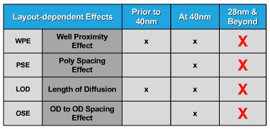
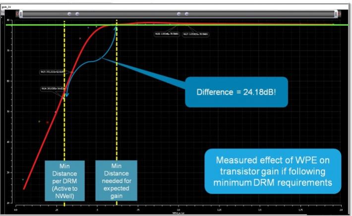

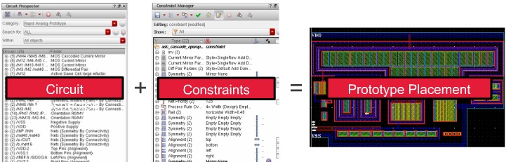
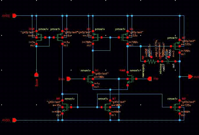
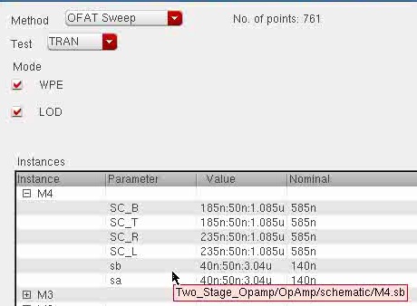
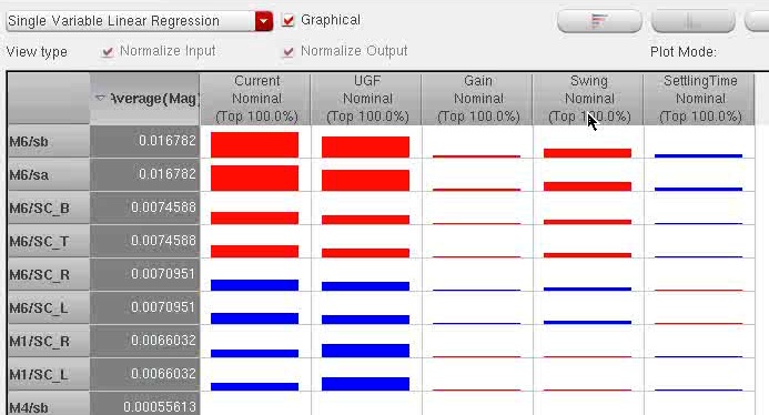
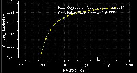


Comments
There are no comments yet.
You must register or log in to view/post comments.