You are currently viewing SemiWiki as a guest which gives you limited access to the site. To view blog comments and experience other SemiWiki features you must be a registered member. Registration is fast, simple, and absolutely free so please,
join our community today!
My IC design career started out with manually sizing transistors to improve performance, while minimizing layout area and power consumption. Fortunately we don’t have to do manual transistor sizing anymore, thanks to EDA tools that are quicker and more accurate than manual methods. MunEDA is an EDA vendor that has developed… Read More
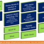
The intricacies of analog IP circuit design have always required special consideration during physical layout. The need for optimum device and/or cell matching on critical circuit topologies necessitates unique layout styles. The complex lithographic design rules of current FinFET process nodes impose additional restrictions… Read More
In the semiconductor ecosystem, several partners (or better to say stakeholders) join together in the overall value chain to finally output the most coveted chip, err I should say SoC these days. It becomes really interesting when we start analyzing the real value added by each of them, none appears to be less. Well, then to whom … Read More
TSMC has been investing in the fabless semiconductor ecosystem for 25+ years and that is why they are the #1 foundry and lead this industry (my opinion). I’m a big fan of joint webinars. Not only is it collaboration open to the masses, it is a close collaboration between the two sponsoring companies. Having worked on the TSMC… Read More
We’ve blogged before about Layout Dependent Effects (LDE) on SemiWiki and how it further complicates the IC design and layout process, especially at 28nm and lower nodes because the IC layout starts to change the MOS device performance. There’s an interesting webinarfrom Cadence on Variation-aware IC Design, … Read More
I already talked about how Cadence is splitting Virtuoso into two. Anyway, it is now officially announced. The 6.1 version will continue to be developed as a sort of Virtuoso classic for people doing designs off the bleeding edge that don’t require the new features. And a new Virtuoso 12.1 intended for people doing 20nm and… Read More
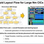
Ciranova presented a hierarchical custom layout flow used on several large advanced-node designs to reduce total layout time by about 50%. Ciranova itself does automated floorplanning and placement software with only limited routing; but since the first two constitute the majority of custom layout time, and strongly influence… Read More
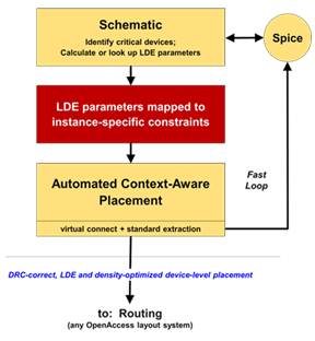
At 28nm and below, a number of electrical variation effects become significant which depend not only on individual devices, but the physical interaction between neighboring devices, wells, etc during the manufacturing process. Some of these effects have become collectively referred to as “Layout Dependent Effects” (LDE);… Read More
Smaller IC nodes bring new challenges to the art of IC layout for AMS designs, like Layout Dependent Effects (LDE). If your custom IC design flow looks like the diagram below then you’re in for many time-consuming iterations because where you place each transistor will impact the actual Vt and Idsat values, which are now a … Read More