
Smaller IC nodes bring new challenges to the art of IC layout for AMS designs, like Layout Dependent Effects (LDE). If your custom IC design flow looks like the diagram below then you’re in for many time-consuming iterations because where you place each transistor will impact the actual Vt and Idsat values, which are now a function of proximity to a well:

Source: EE Times, Mentor Graphics
Analog designs are most sensitive to variations in Vt and current levels, especially for circuit designs that need precise matching.
Engineers at Freescale Semiconductor wrote a paper about Layout Dependent Effects and presented at CICC to quantify how much Vt and Idsat would change based on the location of MOS devices to the edge of a well.
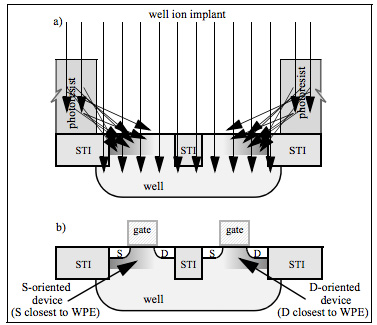
Well Proximity Effect (WPE), Source: Freescale Semiconductor
What they showed was Vt became a function of proximity to the well edge and its value could shift by 50mv:
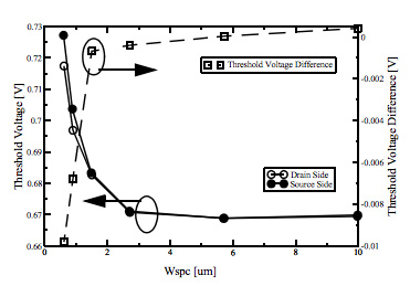
Vt variation. Source: Freescale Semiconductor
Drain current levels can vary by 30% based on proximity to the well edge:
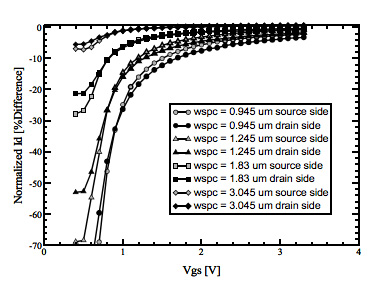
Id variation. Source: Freescale Semiconductor
EDA developers at Mentor Graphics decided to create a different IC design methodology to provide earlier visibility to the IC design team about how LDE is impacting circuit performance. Here’s the new flow:

Source: EE Times, Mentor Graphics
Design constraints about matching requirements are entered at the schematic design state, then fed forward into an LDE estimator module for use during placement. A constraint would define the maximum change in Vt or Id levels between transistors that require matching.
While layout placement is being done the LDE estimator module can quickly determine how each MOS device Vt and Id values are impacted, then compare that to the design constraints provided by the circuit designer, all before routing is started. The layout designer can continue to rearrange transistor placement until all constraints are passing.
Notice how there was no extraction and SPICE circuit simulation required during this LDE estimation phase, the layout designer is interactively placing MOS devices and verifying that the layout is passing or failing the constraints set by the circuit designer.
Test Results
A two-stage Miller OTA amplifier circuit was designed and put through the new methodology.

Schematic capture and layout were done with Pyxis, extraction using Calibre and circuit simulation with Eldo. The target Gain and Bandwidth specs were first met by transistor sizing and circuit simulation, with results shown below:

The first layout iteration was done without the traditional IC flow shown, no LDE estimation was used however the extracted netlist failed both Gain and Bandwidth specs:

Next, layout was done with the LDE estimator module during placement to give the layout designer early feedback on MOS device constraints. The new layout is slightly different from the previous one and most importantly this new layout meets the Gain and Bandwidth specifications:

Here’s a table that summarizes the change in Vt and Id values for each MOS device compared between the first placement and final device placement:

Using the methodology of LDE estimation during placement produced an analog opamp with Vt variations that were up to 10X smaller, and Id variations that were up to 9X smaller.
Summary
Analog circuits are most sensitive to LDE effects, so you need to consider a new methodology to quickly provide feedback on how good your layout is while you are still interactively placing MOS devices instead of waiting until routing, extraction and circuit simulation are completed. This new methodology is all about early feedback which will actually speed up analog design closure.


Comments
6 Replies to “Changing your IC Layout Methodology to Manage Layout Dependent Effects (LDE)”
You must register or log in to view/post comments.