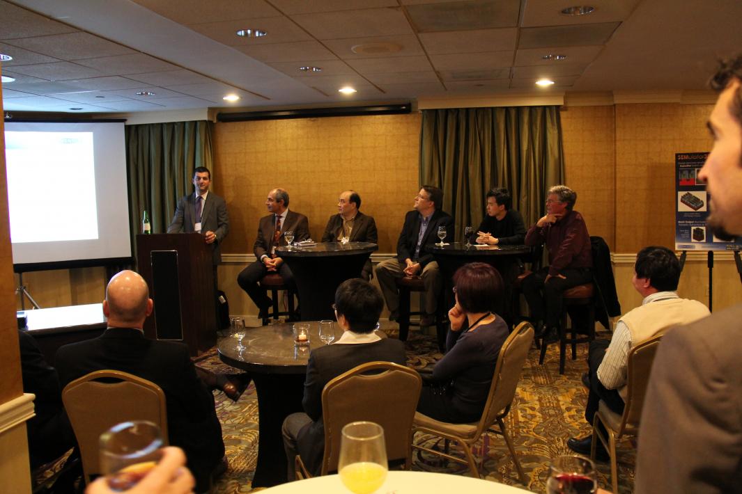
As I see the semiconductor industry going through significant changes and advances, yet ironically plagued by a growing perception that the pace of scaling is slowing, I was inclined to take a peek into what the industry experts say about the state of the industry and the future of Moore’s Law. Fortunately, at last week’s International Electron Devices Meeting (IEDM 2013), a panel discussion among an impressive lineup of experts from industry leading organizations was set up. Dr. David M. Fried, CTO-Semiconductor at Coventor, the host organization, moderated the session.

[Panel – In the Trenches: Insights from Experts on Advanced Technology Development. From left, facing the audience – Dr. David M. Fried (addressing the audience), Dr. Laith Altimime, Dr. Sean Lian, Dr. Brian Greene, Dr. Andy Wei, Dr. Herve Jaouen]
The discussion was structured around defining the greatest technical challenge, and looked further into where to find answers. Generally speaking, the greatest challenge was identified as keeping development of increasingly complex integration schemes on schedule and within budget and how the industry can align to address it. Several panellists added personal details to exemplify the challenge. Dr. Brian Greene, 14nm FEOL architect at IBM, highlighted adoption of new device architectures and materials and increasing process-module interdependencies as challenges. Dr. Sean Lian, Director and Technology Lead at Samsung, is assessing all the schemes to scale down to the 7 nm technology node. Dr. Herve Jaouen, Director of Modelling & Simulation at ST, sees challenges in Middle-of-Line optimization and complex design rules. Dr. Andy Wei, Process Architecture PMTS at GLOBALFOUNDRIES, added that managing patterning costs is a major part of the challenge.
Where to find answers to this challenge? It was a unanimous opinion to find it through closer ties between design and process technology development, industry collaboration, university research and process simulation. There are many variables that must be optimized to keep development on schedule, such as test mask design and optimally allocating resources for fundamental research of advanced technology nodes (e.g. 7nm). Dr. Andy Wei looked up to the EDA tools industry to help meet some of these challenges and accelerate the pace of development.

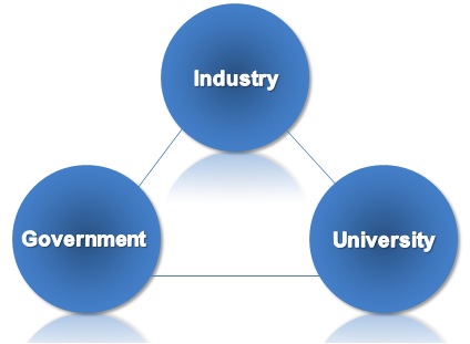
[Collaboration through semiconductor ecosystem, Government and Universities]
How can the industry help? An obvious answer is collaboration within the semiconductor industry ecosystem and with government and research institutions (universities). Dr. Laith Altimime, Director of CMOS Technology & Design at IMEC, stressed that maximizing leverage of the full ecosystem is essential. He referred to this as “The Sum of Minds”. Dr. Brian Greene observed that physical process modelling and advanced inline metrology and defect detection can also help. Also, Dr. Herve Jaouen anticipated that process trials will always help.
I would consider process modelling as crucial help from within the industry ecosystem. And that reminds me about the SEMulator 3D Virtual Fabrication Platform; an innovative solution from Coventor that can address many of these challenges — such as reducing long process-design cycles, long build-and-test learning cycles, vetting process integration ideas, quantifying allowable process module variation and so on. Although it’s off the panel (I wasn’t present in IEDM), it prompts me to ask Dr. David M. Fried certain questions in the context of this discussion –
Q: I think your SEMulator3D tool can help keep the schedule of semiconductor design development, to a large extent. What do you think has to be done more?
A typical silicon learning cycle costs $50M and lasts three months. The industry needs to explore new ways to do things instead of doing the same thing harder and faster. For example, there are an increasing number of big branch decisions during pre-silicon exploration that cannot tolerate this cost or time. Virtual fabrication is a way to take a massive step forward in the rate and pace of silicon development. In early development, virtual fabrication can be used to explore new process ideas in a matter of days instead of months. As the technology approaches manufacturing, virtual fabrication can be used to optimize process control and ramp yield. In both cases, computational time is the only cost.
Q: I see collaborative research either within the industry or with universities can definitely help with advancing the technology and meeting the existing and upcoming challenges. Are you doing some collaboration in that direction to enrich your existing offerings or introduce new offering?
We have numerous on-going university and industry collaborations. We have found that our deepest collaborations benefit both sides most. At the most basic level, getting more minds together is essential to solving the complicated integration issues the industry is faced with today. The deep collaborations lead to understanding technical challenges and delivering solutions faster. Seeing how the industry uses our virtual fabrication platform allows us to continually improve the usability and predictivity of our product.
Q: I know from our earlier discussion that you are working on 3D design rules. To what extent can these rules ease technical challenges for MOL, BEOL or FEOL processes?
We recently released a new functionality called “Structure Search” which evaluates the entire 3D model for structural failure mechanisms. This is an enormous leap forward from the industry’s prevailing method of creating design rules in spreadsheets with limited capability to account for process variation or interactions. The ability to use 3D models that predict exact process variation increases confidence in the design rules and reduces the time required to validate them. Structure Search also enables verification of the special constructs required for designs to leverage the advanced technology nodes we are working on today.
Q: One last question, you say parallel technology tracks such as FinFETs versus FD-SOI makes collaboration difficult. How do you see this in the light that one is simpler and cost effective and the other is complex to process, but may prove to provide better results? Isn’t it worth to validate the results before coming onto a single track?
I don’t think the comparison between those technologies is that cut-and-dry. Both come with their own set of challenges. The division of resources and focus to examine the two technology tracks is another example of how the industry needs to focus on performing development differently. FinFET versus FD-SOI is a big branch decision at the technology level and virtual fabrication should be leveraged here for exploration and comparison. There is still a lot of work ahead to evaluate the two tracks. If there is going to be a clear winner, virtual fabrication is one tool that can decrease the time to make this decision.
It was my great pleasure interacting with Dr. David M. Fried after getting the view from IEDM. This gives a true picture of the way semiconductor technology is going to advance in near future and new ways and tools to help that process. Happy reading!!
More Articles by Pawan Fangaria…..
lang: en_US
Share this post via:


Comments
0 Replies to “Semicon Technology Advancement – A View From IEDM”
You must register or log in to view/post comments.