You are currently viewing SemiWiki as a guest which gives you limited access to the site. To view blog comments and experience other SemiWiki features you must be a registered member. Registration is fast, simple, and absolutely free so please,
join our community today!
Semiconductors are not only critical to modern life, semiconductors are critical to National Security. Now that leading edge semiconductor foundries have left the United States one of the more pressing challenges is secure semiconductor manufacturing. This applies to all countries of course so let’s take a look at the International… Read More
It was 1988 when I got into SPICE (Simulation Program with Integrated Circuit Emphasis)while I was characterizing a 1.5 μm Standard cell library developed by students at my Alma-Mata Furtwangen University in Germany. My professor Dr. Nielinger was not only my advisor he also wrote the first SPICE bible in German language. At that… Read More
An increasing percentage of SoC die area is being allocated to memory arrays, as applications require more data/instruction storage and boot firmware. Indeed, foundries invest considerable R&D resources into optimizing their array technology IP offerings, often with more aggressive device features than used for other… Read More
For me personally EUV has been something of a roller coaster ride over the last several years. I started out a strong believer in EUV but then at the SPIE Advanced Lithography Conference in 2014 TSMC gave a very negative assessment of EUV, and there was a SEMATECH paper on high NA EUV that struck me as extremely unlikely to succeed. I … Read More
While I was at IEDM I had an opportunity to sit down with Subramani (Subi) Kengeri, the Vice President, General Management, CMOS Platforms Business Unit and Jason Gorss from corporate marketing at Global Foundries (GF) for a briefing on GF’s new 22FDX process technology.
Subi told me his background was in design but that he is now… Read More
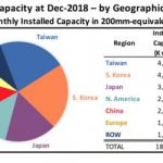
The TSMC quarterly conference call was last week and of course it stirred up quite a bit of controversy. Let me share with you my experience, observations, and opinions and maybe together we can come up with an accurate prediction for 2016. First let’s take a look at 20nm and what people now call the “Apple effect.”
Correct… Read More
For any semiconductor technology node to be adopted in actual semiconductor designs, the very first step is to have a Process Design Kit (PDK) developed for that particular technology node and qualified through several design tools used in the design flow. The development of PDK has not been easy; it’s a tedious, time consuming,… Read More
‘Laughing Buddha’ is eternal, but for semiconductor industry, I must say it’s ‘laughing Moore’. Moore made a predictive hypothesis and the whole world is inclined to let that continue, eternally? When we were at 28nm, we weren’t hoping to go beyond 20/22nm; voices like ‘Moore’s law is dead’ started emerging. Today, we are already… Read More
In the modern semiconductor ecosystem we are seeing rapid advancement in technology breaking past once perceived limits; 28nm, 20nm, 16-14nm, 10nm and we are foreseeing 7nm now. Double and multi-patterning are already being seen along with complex FinFET structures in transistors to gain the ultimate advantages in PPA from… Read More
Last month Cadenceannounced its fastest parasitic extraction tool (minimum 5 times better performance compared to other available tools) which can handle growing design sizes with interconnect explosion, number of parasitics and complexities at advanced process nodes including FinFETs, without impacting accuracy of … Read More