
An SoC can have a collection of multiple blocks and IPs from different sources integrated together along with several other analog and digital components within a native environment. The IPs can be at different levels of abstractions; their RTL descriptions can be in different languages such as Verilog, VHDL, or SystemVerilog.
The design netlist can be in different formats and at different levels. A gate-level netlist can be in Verilog, LEFDEF, or EDIF whereas a transistor-level netlist can be in different forms of Spice. The post-layout parasitic can be represented in several formats including DSPF, RSPF, SPEF, and so on.
Debugging an SoC would mean dealing with all of these formats at different levels of hierarchy in the design along with the design navigation and analysis of source code, simulation waveforms, parasitic, ERC, and so on. Often such analyses at different levels remain disjoint from the main design. What if we had a unified common environment which can take care of all these formats, hierarchical levels, and different forms of analysis within a single cockpit on top of a unified database? That can provide huge productivity and ease of debugging for semiconductor chip designers. The system can do for them automatically what they do manually with several difficult to maintain scripts.
Such an environment was visible when I attended a webinar hosted by Concept Engineering this week. Gerhard Angst, CEO of Concept Engineeringpresented about the capabilities of their StarVision PRO Platform in great detail. This was followed by a detailed demo presented by Pascal Bolzhauser, Product Manager at Concept Engineering.
I could realize that whatever may be the complexity of an SoC, StarVision could trace any part of the SoC and present it in the most simplistic and desired form for a designer to easily understand it, identify any problem, and fix it.

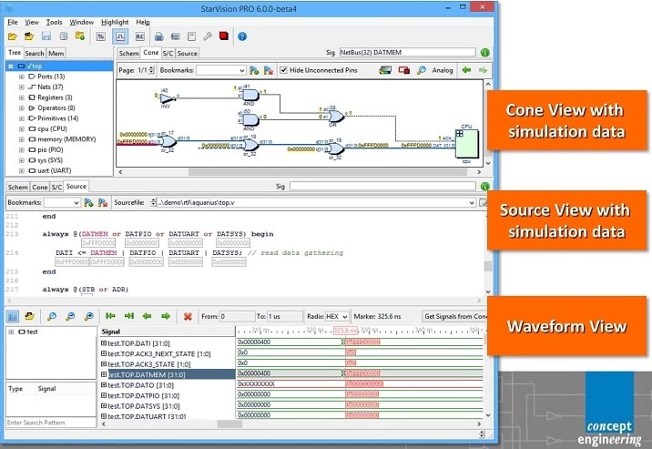
In StarVision PRO platform you can visualize a portion of design schematic in cone view and its corresponding source code view annotated with simulation data along with the actual simulation waveform view. This provides instant clarity on what’s happening with the circuit and where any modification is required.
Connectivity for the full-chip can be easily traced and any IP block can be easily debugged with smart design navigation and analysis at different levels including RTL, gate, transistor, or post-layout parasitic. The platform provides in-built ERC checks which can detect floating signals and other non-conformities. The RTL constructs such as ‘process’ in VHDL and ‘always’ in Verilog can be visualized as blocks in schematic.
This is a versatile environment that supports large digital, analog, or mixed-signal designs. Long critical paths can be explored, interfaces between analog and digital circuits can be identified, and fragments of the circuit can be exported for detailed analysis. Also, users can define their own ERC rules for specific IP or full design. During SoC development, the outputs of tools (such as test insertion and power optimization) that automatically change the design can be exclusively analyzed.
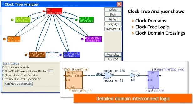
StarVision PRO provides a very intuitive and easy clock domain analysis through color coded clock domain and clock tree visualization. The domain crossings can be visualized by double clicking on interconnections between them. Detailed clock domain analysis can be done in the schematic window in sync with the Clock Tree Analyzer window.
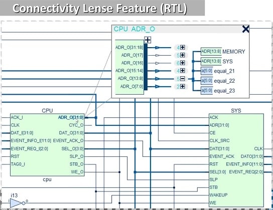
Connectivity Lense is a powerful feature through which you can explore detailed bus connections between components. This feature is available at RTL as well as Spice level.
Similarly, Cone window is an excellent feature through which a port in the schematic can be double clicked to load objects connected to it. One can navigate through multiple levels of hierarchy passing through different levels of design (RTL, gate, or Spice) while staying in the same GUI. This provides a powerful debugging tool for AMS designs.
Also, StarVision PRO has a path extraction engine that can automatically extract and display the path between connected input and output ports. So, input to output connectivity can be quickly checked through this engine.
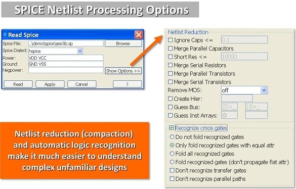
There are several options to simplify complex Spice netlist view and easily understand the underlying CMOS functions. Netlist reduction can be done by turning off parasitic structures or merging resistances, capacitances, and transistors.
A netlist including resistances and capacitances can be visualized and exported for post-layout debugging. RC networks for corresponding wires can be distinguished by applying specific color coding scheme.
A critical path in a complex design can be exported in SPF format which can be separately simulated for detailed path analysis.
StarVision PRO has extremely high performance and capacity to handle large SoC designs. It can load ~3 million devices or gates / minute and ~25000 lines of RTL code / sec. It supports incremental design development where an incomplete block and corresponding RTL code can be supplemented later when available.
The SoC, analog and mixed-signal debugging tools from Concept Engineering are in wide use with more than 130 customers worldwide including 16 out of top20 semiconductor companies. Concept Engineering provides userware APIs which can be used by customers to customize design checks and reports according to their needs.
Ruben Zermeno, Sales Manager at EDA Directwas the organizer of the StarVision PRO webinar. He can be contacted for more information, a demo, or evaluation license at ruben@edadirect.com. For more details about various processing methods in StarVision PRO, visit the page – HERE.
Pawan Kumar Fangaria
Founder & President at www.fangarias.com


Comments
0 Replies to “Multi-Level Debugging Made Easy for SoC Development”
You must register or log in to view/post comments.