You are currently viewing SemiWiki as a guest which gives you limited access to the site. To view blog comments and experience other SemiWiki features you must be a registered member. Registration is fast, simple, and absolutely free so please,
join our community today!
Electrical rule checking (ERC) is a standard part of any design flow. There is a hidden problem with the traditional approach, however. As designs grow in complexity, whether full-custom analog, mixed-signal, or advanced-node digital, the limitations of traditional ERC tools are becoming more problematic. This can lead to… Read More
For its 3rd DAC, Aniah comes to the show with a special treat for its customer : its new Analog Design Assistant, Amigo, makes analog and mixed-signal design engineers more productive every day. This product complements Aniah’s widely deployed, transistor-level verification solution, OneCheck.
Aniah is an EDA startup founded… Read More
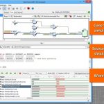
IC designs need to operate reliably under varying conditions and avoid inefficiencies like leakage across power domains. But how do you verify that connections between IP blocks has been done properly? This is where reliability verification, Electrical Rule Checking (ERC) tools and dynamic simulations all come into play particularly… Read More
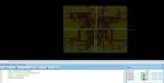
I’ve known about DRC (Design Rule Checking) for IC design, and the same approach can also be applied to PCB design. The continuous evolution of electronics has led to increasingly intricate PCB designs that require Electrical Rule Checking (ERC) to ensure that performance goals are met. This complexity poses several challenges… Read More
Visiting a new EDA vendor at #61DAC is always a treat, because much innovation comes from the start-up companies, instead of the established big four EDA companies. I met with Vincent Bligny, Founder and CEO of Aniah on Wednesday in their booth, to hear about what they are doing differently in EDA. Mr. Bligny has a background working… Read More
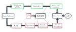
The goal of SoC design teams is to tape-out their project and receive working silicon on the first try, without discovering any bugs in silicon. To achieve this lofty goal requires all types of specialized checking and verification during the design phase to prevent bugs. There are checks at the system level, RTL level, gate level,… Read More
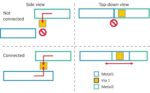
IC designs have physical verification applications like Layout Versus Schematic (LVS) at the transistor-level to ensure that layout and schematics are equivalent, in addition there’s an Electrical Rules Check (ERC) for connections to well regions called a soft check. The connections to all the devices needs to have the most… Read More
An SoC can have a collection of multiple blocks and IPs from different sources integrated together along with several other analog and digital components within a native environment. The IPs can be at different levels of abstractions; their RTL descriptions can be in different languages such as Verilog, VHDL, or SystemVerilog.… Read More
In last 30+ years, the electronic design industry has seen rapid changes more than any other industry. The change has taken place in the whole electronic ecosystem including semiconductor technology, transistor design, IC / SoC design, PCB, and system design. Today, a PCB can be very complex connecting several heterogeneous… Read More
In an electronic world driven by smaller devices packed with larger functions, power becomes a critical factor to manage. With power consumption leading to heat dissipation issues, reliability of the device can be affected, if not controlled or the device not cooled. Moreover, for mobile devices such as smartphones or tablets… Read More