You are currently viewing SemiWiki as a guest which gives you limited access to the site. To view blog comments and experience other SemiWiki features you must be a registered member. Registration is fast, simple, and absolutely free so please,
join our community today!
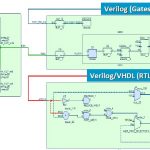
An SoC can have a collection of multiple blocks and IPs from different sources integrated together along with several other analog and digital components within a native environment. The IPs can be at different levels of abstractions; their RTL descriptions can be in different languages such as Verilog, VHDL, or SystemVerilog.… Read More
Starvision Pro from Concept Engineering is a bit like one of those Leatherman multi-tools, it has a huge number of different functions, some of them fairly specialized but nonetheless incredibly useful. Many of these functions are unique to Starvision Pro, with nothing else like it on the market. Some new videos, produced by EDA… Read More
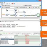
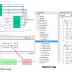
In today’s SoC world where multiple analog and digital blocks along with IPs at different levels of abstractions are placed together on a single chip, debugging at all levels becomes quite difficult and clumsy. While one is working at the top level and needs to investigate a particular connection at an intermediate hierarchical… Read More
In a complex world of SoCs with multi-million gates and IPs from several heterogeneous sources, verification of a complete semiconductor design has become extremely difficult, and it’s not enough. In order to ascertain the right intent of the design throughout the design cycle, debugging at various stages of the design cycle… Read More
In EDA arena we often find companies providing customization platforms along with the tools they offer to their customers. I admire such companies because they equip the end users of a tool to extend its functionality as they like according to their environment, thus increasing the designer productivity significantly. And I’m… Read More
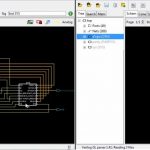
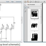
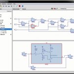
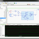
A very popular acronym is ‘WYSIWYG’ – What You See Is What You Get! This is very true and is important to visualize things to make it better in various aspects such as aesthetics, compactness, organization, structure, understandable for correction and so on; the most important, in case of semiconductor design, is being able to identify… Read More
A semiconductor SoC design can have multiple components at different levels of abstractions from different sources and in different languages. While designing an SoC, IPs at different levels have to be integrated without losing the overall design goals. Of course, quality of an IP inside and outside of an SoC must be tested thoroughly.… Read More
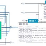
When we talk about parasitic, we talk about post layout design further expanded in terms of electrical components such as resistances and capacitances. In the semiconductor design environment where multiple parts of a design from different sources are assembled together into highly complex, high density SoC, imagine how complex… Read More
When looking at the time to design and verify an SoC we’ve known for many years now that the verification effort requires more time than the design process. So anything that will shorten the verification effort will have the biggest impact on keeping your project on schedule.
A second trend is the amount of Analog content in… Read More
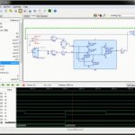
With an HDL-based design methodology many IC engineers code in text languages like SystemVerilog and VHDL, so it’s only natural to use a text-based debug methodology. The expression that, “A picture is worth a thousand words” comes to my mind and in this case a visual debug approach is worth considering for … Read More