You are currently viewing SemiWiki as a guest which gives you limited access to the site. To view blog comments and experience other SemiWiki features you must be a registered member. Registration is fast, simple, and absolutely free so please,
join our community today!
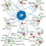
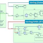
An SoC can have a collection of multiple blocks and IPs from different sources integrated together along with several other analog and digital components within a native environment. The IPs can be at different levels of abstractions; their RTL descriptions can be in different languages such as Verilog, VHDL, or SystemVerilog.… Read More
Although I knew about Crossfire’s capabilities for signing off quality of an IP before its integration into an SoC, there was much more to learn about this tool when I visited Fractal Technologies booth during this DAC. The complexity handled by this tool to qualify any type of IP for its integration into an SoC can be imagined by the… Read More
For any semiconductor technology node to be adopted in actual semiconductor designs, the very first step is to have a Process Design Kit (PDK) developed for that particular technology node and qualified through several design tools used in the design flow. The development of PDK has not been easy; it’s a tedious, time consuming,… Read More
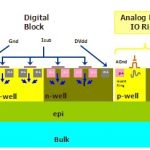
Often substrate noise analysis takes place when everything is there on the chip, but that stage comes near the tape-out which is too late to make major changes in architecture, placement, introducing noise protection circuitry for the victims and so on. It was okay when there used to be very little analog content on the chip. But … Read More
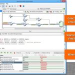
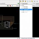
In today’s SoC world where multiple analog and digital blocks along with IPs at different levels of abstractions are placed together on a single chip, debugging at all levels becomes quite difficult and clumsy. While one is working at the top level and needs to investigate a particular connection at an intermediate hierarchical… Read More
Last month Cadenceannounced its fastest parasitic extraction tool (minimum 5 times better performance compared to other available tools) which can handle growing design sizes with interconnect explosion, number of parasitics and complexities at advanced process nodes including FinFETs, without impacting accuracy of … Read More
I think by now a lot has been said about the necessity of multi-patterning at advanced technology nodes with extremely low feature size such as 20nm, because lithography using 193nm wavelength of light makes printing and manufacturing of semiconductor design very difficult. The multi-patterning is a novel semiconductor manufacturing… Read More
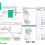
In a complex world of SoCs with multi-million gates and IPs from several heterogeneous sources, verification of a complete semiconductor design has become extremely difficult, and it’s not enough. In order to ascertain the right intent of the design throughout the design cycle, debugging at various stages of the design cycle… Read More
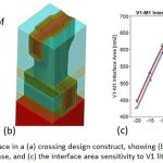
When we talk about parasitic, we talk about post layout design further expanded in terms of electrical components such as resistances and capacitances. In the semiconductor design environment where multiple parts of a design from different sources are assembled together into highly complex, high density SoC, imagine how complex… Read More
In an environment of SoCs with tough targets of multiple functionalities, smallest size, lowest power and fastest performance to achieve within a limited design cycle window in order to meet the rigid time-to-market requirements, any day spent without success becomes very frustrating for a designer. Especially during tape-out… Read More