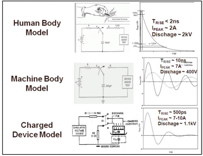
 Electro-static discharge (ESD) has been a problem since the beginning of IC production. Chips function on power supplies of up to a few volts (depending on the era) whereas ESD voltages are measured in the thousands of volts. When you reach out for your car door handle and a spark jumps across, that is ESD. If you were touching a chip instead of your car (and cars contain plenty of chips these days) then the chip has to be able to absorb those thousands of volts and harmlessly dump them without letting voltages or currents on the chip go beyond what can be handled. ESD doesn’t just cause a potential problem when it happens, it can physically destroy the chip. Estimates are that as many as 35% of all in-field chip failures are due to ESD.
For example, if ESD is incorrectly handled and very high voltages end up on the gate of the chip, the discharge can destroy the thin oxide underneath the gate and make that transistor, and probably thus the whole chip, inoperable. Since the thin oxide is getting thinner with each process node it is not surprising that ESD is a problem that is only going to continue to get worse. Metal geometries are also getting smaller, and so have a reduced capacity to handle a current surcharge.
There are other reasons that it is getting worse, not just shrinking geometries. The higher levels of integration on mixed signal chips man that there are many isolated independent power/ground networks, which aggravates the problem. Also, there are more and more hand-held devices (cell-phones etc) which means that there is more direct access to the ICs. You are not very likely to have n ESD problem with the engine-controller in your car since you don’t touch it. The base of your iPhone has a socket with lots of connectors that go straight to the chips inside the phone.
ESD events can also occur during packaging, assembly and test of the IC. And, in fact, charge buildup inside the chip can also cause ESD failures, especially from in-package capacitors and from on-chip memories.
ESD protection has typically been implemented by placing clamp circuits at appropriate locations on the chip that do two things. First, provide a low impedance discharge path for the ESD and second, clamp the signal voltage at a level that avoids dielectric breakdown. Historically these clamp circuits have been placed in the I/O and power/ground pads. Input pads are especially vulnerable since the input pin has to be connected to the gate of the input driver. The clamp circuits are quite large but since the pads and their drivers are already large this doesn’t have a huge impact.
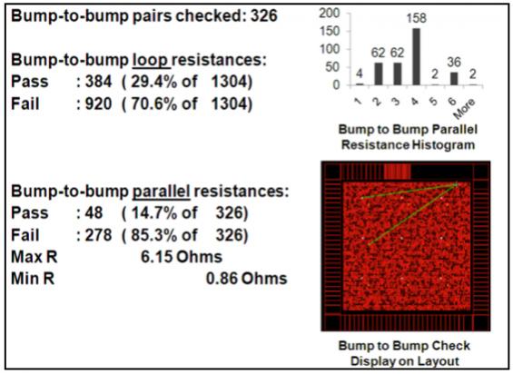
 However, modern designs often have c4 bumps all across the chip, and with the coming of 3D (and 2.5D) designs this will only increase. This means that clamp circuits, which are large, are needed in the core of chip too and thus compete for area with circuitry in the core such as standard cells.
Historically, analysis of ESD has been done in a fairly ad hoc manner, with design guidelines and manual verification. But as the complexity of the design and the number of power/ground nets increases this is no longer adequate. A full-chip ESD verification solution for ESD signoff is required. Indeed, as more ESD protection is needed in the core, it is no longer enough to analyze after the design is complete, ESD protection needs to be planned since it has potentially large impact on the area available in the core for actual implementation of the design.
* Note you must be logged in to read/write comments
Share this post via:


Comments
0 Replies to “Electro-static Discharge (ESD)”
You must register or log in to view/post comments.