IC layout parasitics dominate the performance of custom digital, analog and mixed-signal designs, so the challenge becomes how to identify the root causes and to quantify the effects of parasitics during early design stages. The old method of iterating between layout, extraction, SPICE simulation, followed by manual debug… Read More

Tag: esd
Accelerating Static ESD Simulation for Full-Chip and Multi-Die Designs with Synopsys PathFinder-SC
As analog and mixed-signal designs become increasingly complex, parasitic effects dominate both design time and cost, consuming 30–50% of engineers’ effort in debugging and reanalyzing circuits. Addressing these multiphysics effects requires early verification strategies and reliable simulation solutions. Modern … Read More
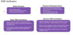
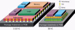
3D ESD verification: Tackling new challenges in advanced IC design
By Dina Medhat
Three key takeaways
- 3D ICs require fundamentally new ESD verification strategies. Traditional 2D approaches cannot address the complexity and unique connections in stacked-die architectures.
- Classifying external and internal IOs is essential for robust and cost-efficient ESD protection. Proper differentiation
Protect against ESD by ensuring latch-up guard rings
By Mark Tawfik
Overview: Protecting ICs from costly ESD and latch-up failures
Electrostatic discharge (ESD) events cost the semiconductor industry an estimated $8 billion annually in lost productivity, warranty claims and product failures [1].
Ensuring the robust protection of integrated circuits (ICs) against various… Read More
Electrical Rule Checking in PCB Tools
I’ve known about DRC (Design Rule Checking) for IC design, and the same approach can also be applied to PCB design. The continuous evolution of electronics has led to increasingly intricate PCB designs that require Electrical Rule Checking (ERC) to ensure that performance goals are met. This complexity poses several challenges… Read More
Aniah and Electrical Rule Checking (ERC) #61DAC

Visiting a new EDA vendor at #61DAC is always a treat, because much innovation comes from the start-up companies, instead of the established big four EDA companies. I met with Vincent Bligny, Founder and CEO of Aniah on Wednesday in their booth, to hear about what they are doing differently in EDA. Mr. Bligny has a background working… Read More
EP177: The Certus Approach to Meeting the Challenges of I/O and ESD with Stephen Fairbanks
Dan is joined by Stephen Fairbanks, CEO of Certus Semiconductor. Stephen is an ESD pioneer with over 30 years of experience starting with his time at Intel, SRF Technologies, and now Certus Semiconductor.
Stephen describes the varied challenges of ESD andI/O library design presented by today’s technologies and design… Read More
Unique IO & ESD Solutions @ DAC 2023!

The semiconductor industry continues to drive innovation and constantly seeks methods to lower costs and improve performance. The advantages of custom I/O libraries versus free libraries can be seen as cost-savings or, more importantly, new markets, new customers, and new business
opportunities.
At DAC 2023, Certus Semiconductor… Read More
CEO Interview: Stephen Fairbanks of Certus Semiconductor

Trained as a semiconductor Analog and RF Circuit Designer, Stephen Fairbanks has been designing and developing process-specific I/O and ESD libraries for 24 years. His foundational training began while attending Brigham Young University designing highspeed 32 GSPS data acquisition systems and RF interfaces for a time-of-flight… Read More
Bizarre results for P2P resistance and current density (100x off) in on-chip ESD network simulations – why?
Resistance checks between ESD diode cells and pads or power clamps, and current density analysis for such current flows are commonly used for ESD networks verification [1]. When such simulations use standard post-layout netlists generated by parasitic extraction tools, the calculated resistances may be dramatically higher… Read More