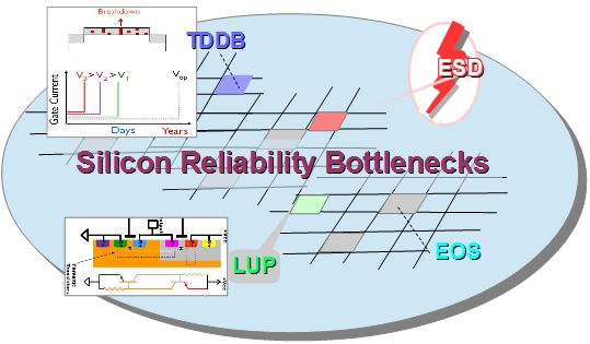
IC reliability is an issue that circuit design engineers and reliability engineers are concerned about, because physical effects like high Current Density (CD) in interconnect layers, or high point-to-point (P2P) resistance on device interconnect can impact reliability, timing or Electrostatic Discharge (ESD) robustness.… Read More

Tag: esd
Magwel Adds Core Device Checking for ESD Verification
In the past ESD sign-off has been accomplished by a combination of techniques. Often ESD experts are asked to look at a design and assess its ESD robustness based on experience gained from prior chips. Alternatively, designers are told to work with a set of rules given to them, again based on previous experience about what usually… Read More
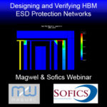
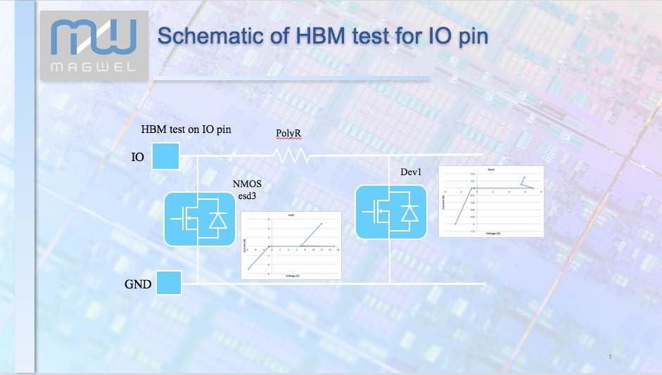
Webinar Replay – Designing and Verifying HBM ESD Protection Networks
Every chip needs ESD protection, especially RF, analog and nm designs. Because each type of design has specific needs relating to IOs, pad rings, operating voltage, process, etc. it is important that the ESD protection network is carefully tailored to the design. Also because of interactions between the design and its ESD protection… Read More
Free Webinar on Verifying On-Chip ESD Protection
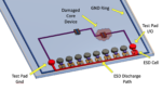
Walking across a carpet can generate up to 35,000 volts of static charge, which is tens of thousands of times higher than the operating voltages of most integrated circuits. When charge build up from static electricity is exposed to the pins of an IC, the electrostatic discharge (ESD) protection network on the chip is intended to… Read More
Webinar of Recent NCTU CDM/ESD Keynote Talk by Dundar Dumlugol – Thursday September 26th

With many design teams still searching for an effective means of identifying Charged Device Model (CDM) issues early in the design process, it comes as no surprise that events on this topic generate a lot of interest and are well attended. In July Magwel’s CEO Dr. Dundar Dumlugol had the honor of being invited by Professor Ming-Dou… Read More
Adding CDM Protection to a Real World LNA Test Case
In RF designs Low Noise Amplifiers (LNA) play a critical role in system operation. They simultaneously need to be extremely sensitive and noise free, yet also must be able to withstand strong signal input without distortion. LNA designers often struggle to meet device performance specifications. Their task is further complicated… Read More
The Flash and the Taiwan ESD Seminar!
During my trip through Asia last week I attended the Taiwan ESD Workshop. Hsinchu is densely populated with some of the smartest semiconductor people in the world so it is well worth the trip, absolutely. As it turns out ESD is one of the top concerns in semiconductor design and manufacture. The current rule based and simulation … Read More
A Practical Approach to Modeling ESD Protection Devices for Circuit Simulation

Lurking inside of every Mosfet is a parasitic bipolar junction transistor (BJT). Of course, in normal circuit operation the BJT does not play a role in the device operation. Accordingly, SPICE models for Mosfets do not behave well when the BJT is triggered. However, these models work just fine for most purposes. The one important… Read More
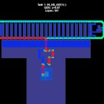
Verifying ESD Fixes Faster with Incremental Analysis
The author of this article, Dündar Dumlugöl, is CEO of Magwel. He has 25 years of experience in EDA managing the development of leading products used for circuit simulation and high-level system design.
Every designer knows how tedious it can be to shuttle back and forth between their layout tool and analysis tools. Every time an… Read More
Electrical Reliability Verification – Now At FullChip
Advanced process technology offers both device and interconnect scaling for increased design density and higher performance while invoking also significant implementation complexities. Aside from the performance, power and area (PPA) aspects, designer is getting entrenched with the need of tackling more reliability … Read More