You are currently viewing SemiWiki as a guest which gives you limited access to the site. To view blog comments and experience other SemiWiki features you must be a registered member. Registration is fast, simple, and absolutely free so please,
join our community today!
Big prototyping hardware is essential to modern firmware and software development for pre-silicon, multi-billion gate hardware. For hardware verification it complements emulation, running fast enough for realistic testing on big software loads while still allowing fast-switch to emulation for more detailed debug where… Read More
Often we hear about isolated instances of excellence from various companies in the semiconductor industry which contribute significantly in building the overall ecosystem. While the individual excellence is essential, it’s rather more important how that excellence is utilized in a larger way by the industry to create a ‘value… Read More
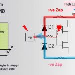
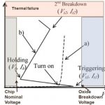
Electro Static Discharge (ESD) has been a major cause of failures in electronic devices. As the electronic devices have moved towards high density SoCs accommodating ever increasing number of gates at lower process nodes, their vulnerability to ESD effects has only increased. Among the reasons for ESD failures in SoCs, device… Read More
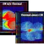
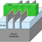
In a world with mobile and IoT devices driven by ultra-low power, high performance and small footprint transistors, FinFET based designs are ideal. FinFETs provide high current drive, low leakage and high device density. However, a FinFET transistor is more exposed to thermal issues, electro migration (EM), and electrostatic… Read More
I think by now there has been good level of discussion on FinFET technology at sub-20 nm process nodes and this is an answer to ultra dense, high performance, low power, and billion+ gate SoC designs within the same area. However, it comes with some of the key challenges with respect to power, noise and reliability of the design. A FinFET… Read More
In the modern semiconductor ecosystem we are seeing rapid advancement in technology breaking past once perceived limits; 28nm, 20nm, 16-14nm, 10nm and we are foreseeing 7nm now. Double and multi-patterning are already being seen along with complex FinFET structures in transistors to gain the ultimate advantages in PPA from… Read More
In this age of electronics, especially with so many different types of human held devices and more upcoming wearable devices, it’s utmost important to protect the massive circuitry inside those tiny parts in the devices from ESD related failures. The protection needs to happen at all stages – cells inside the chips, package… Read More
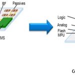
In the semiconductor industry, it feels great to hear about the process technology shrinking to lower nodes along with innovative transistor structures that offer major gains in PPA (Power, Performance and Area). However, it requires huge investment of capital, time and effort from foundries to conceptualize, prototype and… Read More
Do we ever imagine what kind of severe challenges mission critical unmanned systems in air, land and underwater face? They are limited in space and size; have to be light in weight, flexible in different types of operations and at the same time rugged enough to work in extreme climatic conditions. That’s not enough; amidst these … Read More
As Moore’s law keeps going, semiconductor design density on a chip keeps increasing. The real concern today is that the shrinkage in technology node has rendered the small wire geometry and gate oxide thickness (although fine in all other perspectives) extremely vulnerable to ESD (Electrostatic Discharge) effects. More than… Read More