
In this age of electronics, especially with so many different types of human held devices and more upcoming wearable devices, it’s utmost important to protect the massive circuitry inside those tiny parts in the devices from ESD related failures. The protection needs to happen at all stages – cells inside the chips, package and the whole system with special ESD cells connected to external pins to absorb or drain the ESD energy and thus save sensitive internal circuits from damage. Just as an example – if not protected, sensitive internals of an IC can be damaged by even 8V to 10V of discharge, much below the level a human can feel. So, is it possible to look at each cell and protect it and yet not overdesign the circuit? It cannot be done without the help of automated tools; complete analysis at chip (layout, connectivity, metal grid, resistances, substrate etc.), package and system level has to be done, weak spots obtained and fixed, and most importantly ESD signoff done before manufacturing a chip or finalizing the assembly of a system.
Amid ever shrinking geometries, isolated power and ground networks for analog and digital in mixed-signal designs and other complex procedures in SoC designing and packaging, the challenge to protect circuits and systems from ESD has only increased. Read this articlefor more details about the typical challenges of ESD and their solutions. The new trends, tools, demos and ‘how to do tutorials’ are ready to be unveiled in this year’s EOS/ESD Symposiumto be held on 7[SUP]th[/SUP] Sep – 12[SUP]th[/SUP] Sepat Westin La Paloma, Tucson, AZ, USA. A quick look on the agenda tells me about an interesting commercial tutorialoffered by a leader in this domain, ANSYS.
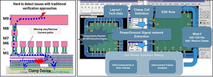
The tutorial (including lecture, presentations and demonstrations) will cover ESD analysis (including identification of HBM, MM and CDM on-chip ESD failures) and solution for complete chip-package-system of a semiconductor design involving ANSYS-Apache suite of tools. The PathFinder, robust silicon proven solution certified by several semiconductor foundries, provides a versatile solution for full-chip level static ESD analysis techniques and block/IP level static and dynamic analysis. It checks the design for its adherence to ESD rules and reports any violation or weak areas such as current density exceeding the limit of a wire or via, inappropriate resistance between pads and clamp cells, active devices and clamp cells or multiple clamp cells, and so on. An easy-to-use GUI environment is provided for debugging the violating paths. This system can also be used for early prototyping and design exploration to trade-off between area and metal routing.
The system also uses other ANSYS tools such as RedHawk and Totem to handle ESD verification and signoff of large SoCs and ANSYS HFSS and SIwave platforms (using chip level ESD models generated by PathFinder) for system level ESD solution.
It’s a nice tutorial to attend to understand and appreciate how ESD issues are uncovered and solved by this set of tools in a complex SoC design and assembly. The tutorial for a complete day is divided in three sections as per following schedule –
Tutorial Day – September 11, 2014
Session 1 – Chip-level Static ESD Analysis – 8:30 AM – 12:00 PM

This session includes full-chip layout based ESD analysis with comprehensive pin-to-pin connectivity checks, resistance checks and interconnects failure analysis along with their root causes. There will be case studies demonstrating hard to detect ESD issues, narrow current paths, missing vias across multiple metal layers and so on.
Session 2 – Dynamic ESD Analysis – 1:00 PM – 2:30 PM
In this session, IP level transient ESD simulation will be explained and shown how it helps in failure analysis. The transient ESD behavior diagnosis and analysis will be discussed which will include modeling of die-level metal grid, substrate network and well-diodes, effective capacitance of package, and pogo pin. Interesting case studies will be presented highlighting how PathFinder uncovered quite involved HBM (Human Body Model) and CDM (Charged Device Model) failures.
Session 3 – System-level ESD Analysis – 3:00 PM – 4:30 PM
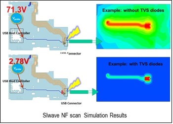
This session will have details about system-level ESD simulation. This will include CECM (Chip ESD Compact Model) generation using PathFinder for system-level ESD analysis and full-wave model generation of ESD gun, ESD protection devices, PCB wires and vias, and connectors using ANSYS HFSS and SIwave. A comprehensive CPS (Chip-Package-System) based dynamic ESD simulation will be run addressing IEC61000-4-2 testing and correlation to silicon measurement.
So, go ahead and register for this tutorial here. Choose option 3 – Symposium plus tutorials or seminars. Check this tutorial flyer for more information about the tutorial.
If you are attending the Symposium, then do not forget to attend these excellent technical paper presentations by experts in the semiconductor industry –
On September 10, 9:00 AM – 10:15 AM
4A.1 HBM Failure Diagnosis on a High-frequency Analog Design with Full-chip Dynamic ESD Simulation
Paul Tong, Anna Tam, Ping Ping Xu, KS Lin, John Hui, Pericom, Inc.
Norman Chang, Bo Hu, Karthik Srinivasan, Margaret Schmitt, ANSYS, Inc.
4A.2 System-Level ESD Failure Diagnosis with Chip-Package-System Dynamic ESD Simulation
Robert (Soungho) Myoung, Norman Chang, ANSYS, Inc.
Byongsu Seol, Samsung Electronics Co., Ltd.
More Articles by Pawan Fangaria…..
Share this post via:


Comments
There are no comments yet.
You must register or log in to view/post comments.