You are currently viewing SemiWiki as a guest which gives you limited access to the site. To view blog comments and experience other SemiWiki features you must be a registered member. Registration is fast, simple, and absolutely free so please,
join our community today!
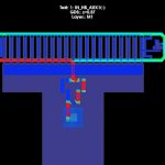
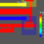
With many design teams still searching for an effective means of identifying Charged Device Model (CDM) issues early in the design process, it comes as no surprise that events on this topic generate a lot of interest and are well attended. In July Magwel’s CEO Dr. Dundar Dumlugol had the honor of being invited by Professor Ming-Dou… Read More
In RF designs Low Noise Amplifiers (LNA) play a critical role in system operation. They simultaneously need to be extremely sensitive and noise free, yet also must be able to withstand strong signal input without distortion. LNA designers often struggle to meet device performance specifications. Their task is further complicated… Read More
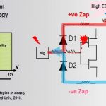
In the realm of ESD protection, Charged Device Model (CDM) is becoming the biggest challenge. Of course, Human Body Model (HBM) is still essential, and needs to be used when verifying chips. However, a number of factors are raising the potential losses that CDM events can cause relative to HBM. These factors fall into two categories:… Read More
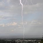
The electrostatic discharge that occurs in lightening, as seen in the picture below, can cause serious damage to the objects on the ground. Over centuries mankind has devised ways, such as lighting rods and arresters, to deflect the energy so it is dissipated harmlessly. The same drama plays out on modern semiconductors due to … Read More
Lurking inside of every Mosfet is a parasitic bipolar junction transistor (BJT). Of course, in normal circuit operation the BJT does not play a role in the device operation. Accordingly, SPICE models for Mosfets do not behave well when the BJT is triggered. However, these models work just fine for most purposes. The one important… Read More
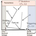
ESD stands for electro-static discharge and deals with the fact that chips have to survive in an electrically hostile environment: people, testers, assembly equipment, shipping tubes. All of these can carry electric charge that has the “potential” (ho-ho) to damage the chip irreversibly. Historically this was… Read More
Electro Static Discharge (ESD) has been a major cause of failures in electronic devices. As the electronic devices have moved towards high density SoCs accommodating ever increasing number of gates at lower process nodes, their vulnerability to ESD effects has only increased. Among the reasons for ESD failures in SoCs, device… Read More
In this age of electronics, especially with so many different types of human held devices and more upcoming wearable devices, it’s utmost important to protect the massive circuitry inside those tiny parts in the devices from ESD related failures. The protection needs to happen at all stages – cells inside the chips, package… Read More
As Moore’s law keeps going, semiconductor design density on a chip keeps increasing. The real concern today is that the shrinkage in technology node has rendered the small wire geometry and gate oxide thickness (although fine in all other perspectives) extremely vulnerable to ESD (Electrostatic Discharge) effects. More than… Read More