You are currently viewing SemiWiki as a guest which gives you limited access to the site. To view blog comments and experience other SemiWiki features you must be a registered member. Registration is fast, simple, and absolutely free so please,
join our community today!
Ansys recently hosted a webinar on reliability signoff for FinFET-based designs, spanning thermal, EM, ESD, EMC and aging effects. I doubt you’re going to easily find a more comprehensive coverage of reliability impact and analysis solutions. If you care about reliability in FinFET designs, you might want to check out this webinar.… Read More
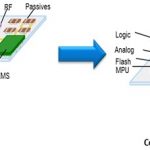
In the largest and fastest growing categories in electronics – mobile, IoT and automotive – analog is playing an increasingly important role. It’s important in delivering high integrity power and critical signals to the design though LDO regulators and PLLs, in managing high speed interfaces like DDR and SERDES, in interfacing… Read More
The way we are seeing technology progression these days is unprecedented. It’s just about six months ago, I had written about the intense collaboration between ANSYSand TSMCon the 16nm FinFET based design flow and TSMC certifying ANSYS tools for TSMC 16nm FF+ technology and also conferring ANSYS with “Partner of the Year” award.… Read More
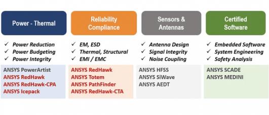
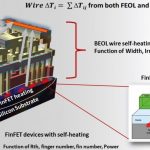
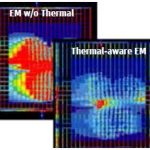
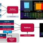
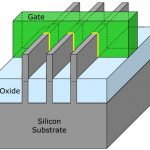
In a world with mobile and IoT devices driven by ultra-low power, high performance and small footprint transistors, FinFET based designs are ideal. FinFETs provide high current drive, low leakage and high device density. However, a FinFET transistor is more exposed to thermal issues, electro migration (EM), and electrostatic… Read More
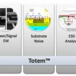
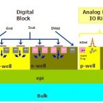
Often substrate noise analysis takes place when everything is there on the chip, but that stage comes near the tape-out which is too late to make major changes in architecture, placement, introducing noise protection circuitry for the victims and so on. It was okay when there used to be very little analog content on the chip. But … Read More
As we move towards packing more and more functionalities and increasing densities of SoCs, the power, thermal and signal integrity issues keep on rising. 3D-IC is a great concept to stack multiple dies on top of each other vertically. While it brings lot of avenues to package dies with multiple functions together, it has challenges… Read More
In the modern semiconductor ecosystem we are seeing rapid advancement in technology breaking past once perceived limits; 28nm, 20nm, 16-14nm, 10nm and we are foreseeing 7nm now. Double and multi-patterning are already being seen along with complex FinFET structures in transistors to gain the ultimate advantages in PPA from… Read More
In this age of electronics, especially with so many different types of human held devices and more upcoming wearable devices, it’s utmost important to protect the massive circuitry inside those tiny parts in the devices from ESD related failures. The protection needs to happen at all stages – cells inside the chips, package… Read More
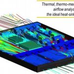
Last week my daughter was playing some games on my Google Nexus smartphone for a while when one of my friends called. When I picked up the phone, I couldn’t imagine it was so hot. There is no doubt; every electronic device today emits an order of magnitude higher heat than what it used to at most a decade ago. There is so much emphasis on … Read More
In the semiconductor industry, it feels great to hear about the process technology shrinking to lower nodes along with innovative transistor structures that offer major gains in PPA (Power, Performance and Area). However, it requires huge investment of capital, time and effort from foundries to conceptualize, prototype and… Read More