In a world with mobile and IoT devices driven by ultra-low power, high performance and small footprint transistors, FinFET based designs are ideal. FinFETs provide high current drive, low leakage and high device density. However, a FinFET transistor is more exposed to thermal issues, electro migration (EM), and electrostatic discharge (ESD) compared to a planar FET. A higher current in FinFET transistor leads to local self heating and a significant increase in substrate temperature. Since the active area in a FinFET is covered by field oxide on three sides, the generated heat is trapped inside. The heat slowly dissipates towards the substrate, thus increasing the substrate temperature. This can lead to domino effect in case of interconnected systems. With high current drive capability of FinFETs, the overall current density of metal interconnects also increases, thus increasing the heat all over. An increase of temperature by 25[SUP]o[/SUP]C can degrade the life of a device by 3x to 5x.
Similarly, with technology scaling the margin between nominal voltage and breakdown voltage of a device is significantly reduced. This leaves very thin operating window for ESD. Also, a FinFET device has very poor snap-back characteristic. Read “Full Chip ESD Sign-off – Necessary” for more details about ESD in devices. Interconnects can be equally vulnerable to large current crowding due to an ESD event.
Considering the FinFET devices to be more prone to such effects which can render them to short-term as well as long-term risks of failure, an SoC design based on FinFET technology nodes cannot be left for EM and ESD sign-offs at the end of the design cycle. It’s advisable to do thermal, EM and ESD analyses of a design as it progresses from very early stages until completion.

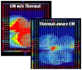
RedHawk from ANSYSprovides a thermal-aware EM analysis platform that can be used as the design progresses. Power and signal EM analyses can be performed at non-uniform temperatures for different metal layers. Temperature profiles generated from ANSYS Sentinel-TI can be annotated on to the RedHawk layout to re-compute the true thermal aware EM violations. This capability is perfect for FinFET based designs which exhibit large variation of temperature across the chip. A detailed description about how Sentinel-TI utilizes RedHawk created CTM (Chip Thermal Model) and analyzes chip-package thermal impact due to leakage and self-heat is provided in a technical paperat techonline website. It also describes about ANSYS Icepak which can be used for system-level thermal analysis.

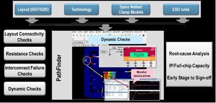
ANSYS PathFinder provides ESD planning, verification and sign-off solution for full-chip SoC as well as IP. It utilizes a simulation based methodology that accurately identifies current density issues and appropriately places diodes and clamps to resolve current bottlenecks in case of an ESD event. An accurate ESD device modeling, flexibility to handle different scenarios and user-friendly debug environment helps designers find route causes for design weaknesses and take appropriate action. Read the technical paper for actual details on ESD analysis and handling.
The paper also describes about different approaches utilized for different types of IP such as standard cell libraries, analog and mixed-signal, I/Os, sensors, PMICs, memories, and so on. For example, Vectorless approach that exercises all nets with accurate switching behavior can be best utilized for a comprehensive EM coverage on power and signal nets inside standard cells. Similarly ANSYS Totem can be used for complex IP such as high-speed I/O, image sensor, and so on.
Today, FinFET node is entering mainstream for IC manufacturing. This expresses the acute need for reliability analysis to become an integral part of the design flow. In order to meet aggressive time-to-market window, the reliability analysis must start as early as possible in the design flow and sign-off at the end for a faster design closure.
Share this post via:


Comments
There are no comments yet.
You must register or log in to view/post comments.