You are currently viewing SemiWiki as a guest which gives you limited access to the site. To view blog comments and experience other SemiWiki features you must be a registered member. Registration is fast, simple, and absolutely free so please,
join our community today!
With every new technology node, there are newer physical effects that need to be taken into account. And every new physical effect brings with itself several new formats to model them. Often a format is also associated with several of its derivatives, sometimes an standard reincarnation of a proprietary format further evolved… Read More
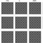
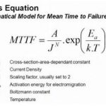
FinFET processes provide power, performance, and area benefits over planar technologies. Yet, a vexing problem aggravated by FinFET’s is the greater local device current density, which translates to an increased concern for signal and power rail metal electromigration reliability failures. There is a critical secondary… Read More
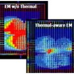
In a world with mobile and IoT devices driven by ultra-low power, high performance and small footprint transistors, FinFET based designs are ideal. FinFETs provide high current drive, low leakage and high device density. However, a FinFET transistor is more exposed to thermal issues, electro migration (EM), and electrostatic… Read More
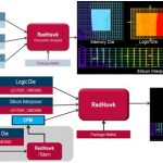
As we move towards packing more and more functionalities and increasing densities of SoCs, the power, thermal and signal integrity issues keep on rising. 3D-IC is a great concept to stack multiple dies on top of each other vertically. While it brings lot of avenues to package dies with multiple functions together, it has challenges… Read More
I think by now there has been good level of discussion on FinFET technology at sub-20 nm process nodes and this is an answer to ultra dense, high performance, low power, and billion+ gate SoC designs within the same area. However, it comes with some of the key challenges with respect to power, noise and reliability of the design. A FinFET… Read More
In this age of SoCs with hundreds of IPs from different sources integrated together and working at high operating frequencies, FPGA designers are hard pressed keeping up the chip reliability from issues arising out of excessive static & dynamic IR drop, power & ground noise, electro migration and so on. While the IPs are… Read More
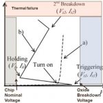
As Moore’s law keeps going, semiconductor design density on a chip keeps increasing. The real concern today is that the shrinkage in technology node has rendered the small wire geometry and gate oxide thickness (although fine in all other perspectives) extremely vulnerable to ESD (Electrostatic Discharge) effects. More than… Read More
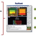
Invarian is an interesting EDA company that sees a niche market opening in the physical verification space. There are a number of converging factors driving this opportunity. Electromigration and voltage-drop for full-chip analysis demands SPICE level accuracy with fast runtimes. Invarian solves that problem with macro … Read More