

In the world of electronic systems design, complexity has always been a major challenge. As technology advances and demands for more efficient and powerful electronic devices grow, engineers face increasingly intricate design requirements. These complexities often lead to longer design cycles, increased costs, and potential design flaws. Siemens EDA recognizes the urgent need for innovative solutions to overcome these obstacles. The company has identified artificial intelligence (AI) as a technology that could offer tremendous leverage for innovation. AI encompasses computational technologies that enable machines to reason and infer without human intervention. AI solutions can analyze large volumes of data to identify patterns and trends, improving processes and providing recommendations for better decision-making.
Siemens EDA has been making significant investments in AI technologies and applying them to various product areas, including PCB design, autonomous driving systems, smart factory floor management and smart city management. The company recently published a whitepaper that delves into how the application of AI technology can address the challenges in printed circuit board (PCB) design.
Challenges in PCB Design
PCB electronic systems engineers face challenges in designing complex, fast ICs that require adequate power, cooling, signal integrity, and thermal integrity. They must deliver high-performance PCBs and interconnected electronic systems within shrinking time-to-market windows while minimizing power consumption. Understanding PCB design and EDA tools involves a steep learning curve and engineers often learn on the job. Component selection is another challenge that requires extensive research and analysis of datasheets.
Leveraging AI
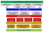
AI can mine completed designs to identify patterns and guide designers to the next logical step, improving design quality and efficiency. AI can develop models based on historical information to recommend viable component options, speeding up the selection process. Integrate this with real-time visibility into component supply chain and it turns into a powerful capability.
The ultimate goal of AI-driven electronic design is for AI algorithms to generate PCB designs and manufacturing outputs, reducing design time and eliminating costly mistakes.
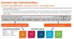
Generative Design
Generative design is an innovative approach that uses algorithms and computational methods to automatically generate and optimize design solutions based on specified parameters and constraints. It combines the power of artificial intelligence, machine learning (ML), deep learning (DL) and advanced simulation techniques to explore a vast design space and produce optimized and efficient designs.
Benefits of Leveraging AI in Electronic Systems Design
Generating component models, such as symbols, physical geometries, and simulation models, is time-consuming. AI technologies like natural language processing and image recognition can automatically process datasheets and generate the required models, reducing manual effort and leveraging domain knowledge.
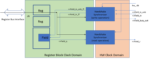
Schematic connectivity, establishing connections between components, is another manual task. ML models trained on completed designs can recommend components and suggest pin-to-pin connections, accelerating the design process.
Dynamic reuse of functional blocks and intelligent database management can be achieved by training DL models, enabling design tools to predict potential functions of blocks and suggest reusable placement and routing options.
Constraints, such as layout, high-speed design, manufacturing, and test rules, are usually entered manually, posing a risk of errors. AI can recommend constraint sets and values based on the current design and knowledge from released designs, streamlining the process.
Layout tasks like component placement and routing are time-consuming. AI systems can recommend placement and routing strategies based on completed designs, and advanced routing methodologies like sketch routing can be applied. Auto routing and analysis tools can also benefit from AI/ML algorithms to generate optimal routes and perform accurate simulations.
Summary
AI is increasingly important in enhancing operational productivity and user expertise. In PCB design, AI is particularly valuable in automating manual processes and enabling entry-level users to perform tasks that previously required expert knowledge. By leveraging AI technologies, decision-making can be accelerated, mundane processes can be automated, new users can work more efficiently, and the performance and manufacturability of multi-domain systems can be optimized.
As part of the Siemens Xcelerator portfolio, AI-driven tools enable electronic systems design companies to leverage AI technologies and bring futuristic products to market. Siemens continually identifies new use cases where AI can be applied to improve design tools and invests time and resources in enhancing existing algorithms or developing innovative methodologies to address challenges.
This whitepaper is a valuable read for everyone involved in the electronic systems design process.


