PCI Express (PCIe), PCIe switches, Time Division Multiplexing (TDM), Network Interface Cards (NICs), and SmartNICs are all well-established technologies that have formed the backbone of computing and networking systems for years. More recently, SuperNICs have emerged as the next generation of networking devices optimized for AI infrastructure.
What has changed is not the technology itself, but the demands placed upon it. As artificial intelligence (AI) and high-performance computing (HPC) systems scale from a handful of accelerators to thousands, and even hundreds of thousands of interconnected GPUs, efficient communication has become just as important as computational performance. In today’s AI clusters, moving data quickly and predictably between compute, memory, storage, and networking resources is often the key to overall system performance.
Strategic Importance of Connectivity
This shift has transformed connectivity from an enabling technology into a strategic differentiator. Rather than replacing proven standards, the industry is extending them with architectural innovations that improve bandwidth utilization, scalability, and flexibility for AI workloads.
The growing importance of interface technologies is reflected in the industry’s increasing focus on market intelligence. For years, IPnest (now part of SemiWiki), has reported the evolution of the interface IP market through its annual Interface IP Survey report, providing one of the industry’s most comprehensive analyses of technology trends, vendor positioning, and market growth. The report underscores the rapid expansion of connectivity IP, driven by AI and high-performance computing.
According to the recently published Interface IP Survey report by SemiWiki, Rambus achieved 29% year-over-year growth in its PCIe interface IP business, highlighting its growing presence in the high-speed connectivity IP market. Building on this momentum, Rambus has introduced PCIe 7 Switch IP with integrated Time Division Multiplexing (TDM), designed to address the communication challenges of next-generation AI networking SoCs.
AI is Redefining Connectivity
As AI infrastructure grows in size and complexity, simply adding more GPUs is no longer enough. Modern AI systems combine CPUs, GPUs, storage, networking devices, SmartNICs, SuperNICs, and CXL memory expanders, all of which must communicate continuously across a shared interconnect fabric.
This makes connectivity a critical determinant of system performance. Even the most powerful accelerators cannot deliver maximum throughput if data cannot move efficiently between system resources.
PCI Express continues to serve as the backbone of this communication infrastructure, but higher bandwidth alone is only part of the solution.
PCIe 7.0: More Than Higher Bandwidth
PCIe 7.0 doubles the data rate from 64 GT/s to 128 GT/s per lane, providing the bandwidth needed for increasingly data-intensive AI workloads.
However, as bandwidth increases, so do the challenges. Efficiently sharing bandwidth among many simultaneously active devices, maintaining predictable latency, and avoiding communication bottlenecks become just as important as increasing raw throughput.
This is where advanced PCIe switch architectures play a critical role.
PCIe Switches Take Center Stage
PCIe switches have existed since the earliest generations of PCI Express, enabling scalable communication between processors and peripheral devices. Their importance has grown dramatically with AI, where direct connections between every processor and every accelerator are no longer practical.
Today, PCIe switch IP is increasingly embedded within advanced networking SoCs used in SmartNICs and the emerging class of SuperNICs. These devices sit at the convergence of compute, storage, networking, and AI acceleration, enabling efficient communication across large-scale AI clusters.
While SmartNICs primarily offload infrastructure functions such as networking, storage, security, and virtualization, SuperNICs are purpose-built for AI, supporting high-performance communication among thousands of GPUs and accelerators operating in tightly synchronized training environments.
Time Division Multiplexing Improves Bandwidth Efficiency
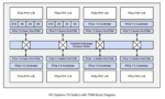
One of the key innovations in the Rambus PCIe 7 Switch IP is the integration of Time Division Multiplexing (TDM). Importantly, TDM is not part of the PCIe 7.0 specification; it is an architectural enhancement implemented within the switch itself.
Rather than assigning fixed bandwidth to connected devices, TDM dynamically allocates transmission opportunities based on application demand. This improves link utilization, enables more efficient resource sharing, and helps maintain predictable traffic behavior as workloads change.
The switch architecture also provides flexible PCIe lane partitioning. A x16 interface, for example, can be configured during system initialization as one x16 connection, two x8 connections, or four x4 connections, allowing system designers to adapt the same hardware platform for different combinations of GPUs, SSDs, accelerators, and networking devices.
Optimized for AI Networking SoCs
Rambus designed its PCIe 7 Switch IP specifically for the implementation challenges of modern AI networking chips. In addition to supporting PCIe 7.0 data rates and integrated TDM, the architecture is physically aware, enabling more efficient implementation across the large silicon dies commonly found in advanced SmartNIC and SuperNIC SoCs.
This system-level approach addresses not only protocol functionality but also practical challenges such as routing complexity, latency, and physical implementation.
Summary
The future of AI infrastructure will depend not only on more powerful processors, but also on the intelligent connectivity that allows them to operate as one coherent, high-performance system.
PCIe, PCIe switches, NICs, SmartNICs, and TDM underpinning modern connectivity not new technologies per se. What is new is the role they play in enabling the scale and performance demanded by AI and HPC.
As AI systems continue to expand, innovation is increasingly focused on making these proven technologies work smarter rather than simply faster. PCIe 7.0 provides the bandwidth, while architectural enhancements such as Rambus’ PCIe 7 Switch IP with integrated Time Division Multiplexing help ensure that bandwidth is used efficiently, flexibly, and predictably.
A short overview video from Rambus.
Download Rambus PCIe 7.0 Switch with TDM product brief from here.
Also Read:
Rambus Delivers Complete DDR5 Client Chipset for High-Speed CUDIMM and CSODIMM Memory Modules
WEBINAR: HBM4E Advances Bandwidth Performance for AI Training
How Memory Technology Is Powering the Next Era of Compute