Mark Ren has 26 years of EDA and AI R&D experience spanning IBM Research and NVIDIA Research, driving design automation innovations that power modern chip design. He received the IBM Corporate Award for contributions to the design closure for high-performance microprocessors. At NVIDIA, he helped establish the company as a world leader in AI for chip design and GPU-accelerated EDA. Mark has spearheaded the modern GPU-accelerated EDA movement, driving adoption of deep-learning frameworks to unlock performance and scalability for EDA workloads. He also led the first industrial LLM-for-chip-design effort, ChipNeMo.
His work spans design automation across digital, analog, and PCB, and has been recognized with two DAC Best Paper Awards and 10+ Best Paper Awards /nominations across major EDA conferences. Mark has delivered keynotes for Cadence, Synopsys, TSMC, Intel, and Silicon Labs. He has taught AI-for-chip-design tutorials at DAC and Hot Chips, served as Chair of the LLM Aided Design Conference and is on the steering/organizing committees for ICCAD and ISPD. He is an IEEE Fellow, and his work has been covered by publications such as WIRED, Fortune, and EE Times.
Tell us about your company
Agentrys is an applied research team building the future of chip design. We are pioneering Agentic Design Automation (ADA), a new paradigm for semiconductor engineering. Electronic Design Automation (EDA) has transformed the industry by automating engineering algorithms. Today, frontier AI can automate many engineering tasks by understanding specifications, generating RTL and scripts, creating assertions and testbenches, and assisting with debug.
We believe the next transformation is to automate and continuously improve the engineering workflows that determine product quality, engineering productivity, and time-to-market. This transformation will result in an agentic engineering workflow customized to each design team’s own engineering knowledge and design methodology. We call this Agentic Design Automation (ADA).
Our mission is to help every semiconductor company create its own continuously improving agentic engineering workforce. The Agentrys Studio delivers a platform that enables engineering organizations to build, deploy, evaluate, and continuously improve that workforce, running securely on the company’s existing EDA infrastructure and learning from its own engineering data.
Agentrys includes researchers and engineers from NVIDIA, Meta, AMD, Samsung, Google, Siemens, and other leading technology companies.
What problems are you solving?
Contemporary chip development depends on long-running, complex, repeatedly executed engineering workflows that demand significant manual effort and engineering judgment. Examples include verification closure, physical implementation, timing closure, analog layout optimization, design-space exploration, and signoff.
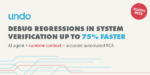
Even though EDA tools have automated many parts of these workflows, significant engineering effort is still required to achieve high-quality results. For example, debug dominates verification time, floor planning gates physical design, and layout remains difficult for analog circuits.
General AI and commercial agents will increasingly automate many engineering tasks by writing code, generating scripts, answering questions, analyzing logs, debugging, and more. However, solving these complex workflows at expert design quality is still out of reach.
Our goal is to help design teams automate these workflows and keep improving them, eventually surpassing expert-level design capability.
What application areas are your strongest?
Our platform is designed to span the semiconductor development lifecycle, but we are deliberately focused. Our strongest and most proven area today is functional verification — testbench stimulus generation, checker generation, and assertion creation.
On the verification tasks of NVIDIA’s public CVDP (Comprehensive Verilog Design Problems) benchmark, our system reaches roughly 95% on both checker generation and assertion generation, and 90% on testbench stimulus generation. These are measurable, published results on a benchmark our own team helped create.
Next, we are extending into physical implementation and optimization, where we are already in active customer engagements. Our roadmap covers RTL design, analog design, and system design.
Rather than shipping isolated point tools, we deliver Agentrys Studio, giving design teams one platform to build continuously improving capability across multiple engineering domains. This allows a team’s agents to become a compounding, crossflow asset rather than a collection of disconnected tools.
What keeps your customers up at night?
Every semiconductor company is wrestling with the same questions. How do we use AI to improve engineering productivity — safely, and inside our existing flows? How do we protect proprietary engineering knowledge when our designs are our most valuable asset? How do we deploy AI inside secure, often air-gapped, enterprise environments?
And the deepest question: if every competitor adopts similar frontier AI, where does lasting advantage come from? If AI is just another productivity tool everyone buys off the shelf, it raises the floor for the whole industry but gives no one an edge.
Our answer is that the advantage must come from something a team owns — its methodology and its data. So, the agents should be yours. They should learn from your designs, run behind your firewall, and get better with every project. That is the difference between renting capability everyone else can rent and building an asset that compounds for you alone.
What does the competitive landscape look like and how do you differentiate?
The industry is moving rapidly. Frontier-model providers, commercial AI agents, EDA vendors, and startups are all bringing AI into semiconductor engineering. We see that as validation that AI will become a standard component of chip design.
Major EDA companies provide AI capabilities on top of the tools they sell. Some AI-for-chip-design startups focus on building foundation models for chip design. Others focus on domain-specific AI agents, and internal AI teams within design organizations are building their own agents with the help of coding agents such as Codex and Claude Code.
Our view is that the core problem to solve is how effectively an engineering organization builds, deploys, evaluates, and continuously improves the engineering workflows that define its products.
That philosophy drives several architectural decisions.
Agentic Design Automation Platform: We provide Agentrys Studio rather than a fixed collection of vendor-controlled agents. This platform combines frontier models with a self-evolving agent infrastructure, agent-native tools, and customizable AI models and domain knowledge to automate complex design workflows and learn from existing design data.
Customer Ownership: Customers build an agentic engineering workforce that evolves around their own workflows, methodology, engineering knowledge, and design data. We deploy inside the customer’s environment, either on-prem or in a private cloud. The RTL, netlists, PDKs, verification collateral, and engineering knowledge remain under the customer’s control.
Cross-vendor by design: Production engineering workflows span commercial EDA tools and agents from multiple vendors as well as internal tools and infrastructure. We orchestrate across that heterogeneous environment instead of assuming a single tool ecosystem.
What new features or technologies are you working on?
We are expanding Agentrys Studio along several dimensions: enterprise on-premise deployment, workflow orchestration for long-running engineering processes, grounded engineering evaluation, engineering knowledge management, and continuous optimization through our Self-Evolve framework. A major area of innovation is agent-native tooling.
Traditional EDA tools are designed for human engineers. They provide interfaces, controls, and feedback optimized for interactive engineering. AI agents require a different interaction model. These tools need machine-actionable APIs and engineering feedback that enable autonomous reasoning, rapid iteration, and continuous optimization.
Agent-native tooling complements commercial EDA by providing AI agents with the interfaces and feedback needed to solve long-running, complex engineering workflows more effectively. Rather than replacing existing EDA tools, it works alongside them to make AI-driven engineering more capable.
We are also advancing our Self-Evolve framework, which continuously evaluates engineering outcomes against grounded references and customer-defined acceptance criteria. Every workflow execution generates engineering observations that improve agents, workflows, engineering knowledge, and tooling over time.
Our long-term vision is to give every semiconductor company a continuously improving agentic engineering workforce that becomes more capable with every project, while preserving the security, methodologies, and engineering knowledge that make each organization unique.
How do customers normally engage with your company?
Engagements usually follow three steps — we call it Onboard, Evolve, Scale.
The process starts with a technical discussion of the customer’s workflows and AI strategy, where we identify one or two high-value workflows with measurable targets. We then onboard that real flow, integrating with the customer’s existing EDA tools, knowledge, and infrastructure, on-prem. We operate in the customer’s methodology rather than requiring them to re-implement it in ours.
From there, the agents evolve by adapting to how the team designs and become more correct on the team’s own designs with each run, measured against grounded references. As confidence grows, customers scale ADA across additional workflows and engineering teams.
That arc is also our business model. Onboard to land, evolve to earn trust, scale across the organization. Today we are engaged with customers across both front-end design and physical design, from tier-1 semiconductor companies to AI-silicon startups looking to scale small teams with agentic automation.
CONTACT AGENTRYS AI