You are currently viewing SemiWiki as a guest which gives you limited access to the site. To view blog comments and experience other SemiWiki features you must be a registered member. Registration is fast, simple, and absolutely free so please, join our community today!
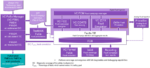
Electronic Design Automation, or EDA, is the software infrastructure that transforms a hardware specification into a manufacturable integrated circuit. At advanced process nodes, the problem is no longer simply drawing transistors or connecting gates. A modern system-on-chip contains billions of standard cells, hundreds of clock and power domains, dense SRAM macros, high-speed interfaces, embedded analog blocks, and often chiplet or advanced-package integration. EDA tools manage this complexity by converting register-transfer level descriptions into optimized physical layouts while proving that the resulting design satisfies functional, electrical, timing, and manufacturing constraints.
The flow begins with RTL written in Verilog, SystemVerilog, or VHDL. Logic synthesis maps this RTL into a gate-level netlist using a process-specific standard-cell library. The synthesis engine must optimize Boolean logic under timing, area, power, and testability constraints while respecting library characterization across process, voltage, and temperature corners. For high-performance designs, synthesis is not a single pass. Engineers iterate constraints, clock definitions, hierarchy boundaries, retiming options, and physical-awareness settings to reduce critical-path delay before physical implementation.
Physical design then converts the netlist into layout. Floorplanning defines macro placement, power grids, clock topology, voltage islands, and routing resources. Placement engines position millions or billions of instances while minimizing wirelength, congestion, timing violations, and power density. Clock-tree synthesis inserts buffers and balances skew across clock domains. Routing tools assign interconnect across many metal layers while obeying spacing, width, via, electromigration, multi-patterning, and density rules. At leading-edge nodes, routing is constrained by thousands of design rules, and local layout decisions can affect yield, timing, IR drop, and signal integrity simultaneously.
Signoff analysis verifies that the physical implementation is electrically robust. Static timing analysis checks setup and hold closure across many PVT scenarios, extracted parasitics, clock uncertainties, and on-chip variation models. Parasitic extraction calculates resistance, capacitance, and coupling effects from the final routed layout. Power integrity tools evaluate dynamic and static IR drop, electromigration, and local current density. Signal-integrity analysis checks crosstalk-induced delay shifts and noise. These analyses are interdependent: fixing timing can worsen congestion, reducing IR drop can increase area, and changing routing can alter parasitics enough to reopen timing violations.
Functional verification is usually the largest engineering workload. Simulation runs directed and constrained-random tests against RTL and gate-level models. Formal verification proves equivalence between RTL and synthesized netlists, checks protocol properties, and validates unreachable-state assumptions. Coverage tools track exercised states, transitions, assertions, and functional scenarios. For large SoCs, hardware emulation maps the design onto specialized hardware so firmware, drivers, operating systems, and system workloads can run before silicon returns. This is essential for AI accelerators and datacenter processors, where full-stack validation requires interactions among compute arrays, memory controllers, interconnect fabrics, PCIe, CXL, HBM, security engines, and software runtime layers.
Physical verification is the final manufacturing gate. Design rule checking verifies compliance with foundry geometry constraints. Layout-versus-schematic comparison proves that the mask layout implements the intended circuit. Antenna checks, density checks, lithography-aware checks, and reliability checks reduce manufacturing and lifetime-failure risk. The final output is a GDSII or OASIS database delivered to the foundry for mask generation and wafer fabrication.
The engineering lock-in in EDA comes from flow dependency. Tool outputs are not isolated artifacts; each stage feeds constraints, models, reports, and databases into the next. A change in synthesis can alter placement. A placement change can affect routing. Routing changes modify parasitics. Parasitic changes can break timing, power integrity, or signal integrity. Because of this dependency graph, design teams build extensive internal scripts, regression systems, signoff checklists, and debug methodologies around specific toolchains.
Bottom line: The technical value of EDA is therefore not just automation. It is convergent optimization under extreme constraint density. The tools must search enormous design spaces while producing results that are functionally correct, timing-clean, power-compliant, manufacturable, and economically competitive. As process nodes shrink and systems move toward chiplets, advanced packaging, and AI-driven design-space exploration, EDA is becoming an integrated optimization platform spanning RTL, silicon, package, board, thermal, electromagnetic, and system-level verification.
Over the last year, the EDA industry has started using a new vocabulary: agents, super agents, mental models, native skills, playbooks, RAG, MCP, autonomous workflows, and AI-first design.
The language is new, but the motivation is familiar to anyone who has worked in chip design.
Design complexity keeps increasing. The number of tools in the flow keeps increasing. Logs, reports, waveforms, constraints, schematics, layouts, and verification artifacts keep multiplying. Meanwhile, engineering expertise remains the bottleneck. Analog and mixed-signal design feel this even more sharply than digital because so much of the work depends on topology intuition, device-level tradeoffs, layout sensitivity, and a long sequence of judgment-heavy iterations.
The recent announcements from Cadence, Siemens EDA, and Synopsys therefore matter. They are not simply another generation of AI assistants. They signal an architectural shift: from AI as a helper sitting beside EDA tools toward AI as an orchestration layer that can plan, call tools, interpret results, and iterate.
At the same time, I think we should be careful about what problem has actually been solved.
The current wave is impressive, but it is not yet the same as a persistent, learning, correctness-aware analog design intelligence system. Most public material still points to systems that are strong at workflow orchestration and tool invocation, but less explicit about deep graph-native circuit reasoning, long-horizon design memory, cross-design learning, and correctness propagation inside the optimization loop.
This distinction matters. Teaching an AI system to run an engineering workflow is not the same thing as teaching it to accumulate engineering judgment. For analog design especially, that judgment is learned not only from design artifacts, but from the sequence of decisions, experiments, failures, and recoveries that produced them.
This post is my attempt to place the current state of the art on a few technical dimensions — especially from the perspective of analog and custom design, and then outline the research directions that seem most promising.
Chatbots and beyond
A good place to start is by recognizing what these systems are not. They are not simply LLM wrappers. Cadence’s AgentStack and AI Super Agents, Siemens EDA’s Fuse EDA AI Agent, and Synopsys’ AgentEngineer all point toward a common direction: AI systems that can decompose engineering goals into tool-grounded actions, coordinate workflows across multiple stages of the design process, interpret results, and iterate toward objectives.
The details differ, but the underlying architectural shift is remarkably consistent. Across all three vendors, the center of gravity is moving from “AI answers a question” toward “AI coordinates engineering work”.
That is, unmistakably, a major step forward. The more interesting question, however, is whether workflow coordination is the endpoint — or merely the foundation for something deeper.
To answer that question, it helps to examine today’s agentic EDA systems along a few dimensions that, in my view, distinguish workflow automation from genuine design intelligence.
Dimension 1: Flow Coverage
The strongest public claims today are around flow orchestration.
Cadence presents one of the clearest decompositions: ChipStack for RTL design and verification, ViraStack for analog design and verification, and InnoStack for implementation and signoff. Siemens positions Fuse across a broad engineering landscape spanning architecture, custom IC, verification, physical implementation, manufacturing, and PCB workflows. Synopsys similarly describes agent collaboration across RTL generation, verification, planning, and engineering automation.
On the flow-coverage dimension, the industry has clearly crossed a critical threshold. The ambition is no longer isolated sizing, isolated testbench generation, or isolated log triage. The ambition is full-flow coordination.
But broad flow coverage is not the same thing as deep design cognition.
For digital implementation, much of the state already exists in formalized artifacts: RTL, constraints, timing graphs, floorplans, and signoff reports.
For analog design, the most significant state often lives somewhere else. It lives in the designer’s understanding of:
why a topology was chosen
why a device was biased that way
which failure mode is suspected
which tradeoffs have already been explored
which paths were abandoned weeks ago
Automating analog flow steps is valuable. But analog expertise is accumulated through successive design iterations, not isolated tool executions. Externalizing and ultimately compounding that design cognition is a much harder problem.
Dimension 2: Memory and Design Context
This is where the public systems start to diverge.
Cadence’s Mental Model concept is particularly interesting because it recognizes that agents need structured representations of design intent rather than relying entirely on prompt context. Siemens discusses RAG, EDA-specific parsers, Agent Skills, and executable playbooks. Synopsys emphasizes systems that learn and improve through feedback. All of these are important developments. The key question, however, is whether these architectures are primarily contextual, or whether they actually learn from design evolution.
Contextual memory answers questions such as:
What is the current design?
What is the current specification?
What simulation result did we just obtain?
What existing IP looks similar?
Evolutionary memory answers a different set of questions:
What did we try?
Why did we try it?
What changed?
Which metrics improved?
Which metrics regressed?
Which failure modes repeated?
Which designer overrides proved correct?
Which fixes consistently worked across designs?
For analog design, the second category is often more consequential than the first. A design is not merely a netlist plus constraints. It is the outcome of a trajectory through a high-dimensional tradeoff space — a sequence of hypotheses, design decisions, simulations, failures, corrections, and refinements. Preserving that trajectory may ultimately be more valuable than preserving the final artifact alone.
I find the concept of a Design Evolution Graph particularly compelling. Every iteration becomes a transition: ‘State Sₙ → Action → State Sₙ₊₁’with measurable deltas in performance, correctness, yield, power, area, robustness, and physical feasibility. Over time, those transitions become the raw material for a reusable Pattern Library of failure modes, fixes, tradeoffs, and convergence strategies. Without explicit evolution memory, an agent may become highly effective within a single session while still failing to accumulate knowledge across months, projects, and topology families.
If Design Evolution Graphs capture how a design changes over time, the next question is whether an AI system truly understands what it is changing.
Dimension 3: Reasoning Over Analog Structure
The public vendor systems appear strongest where they can ground LLM behavior in tools, skills, and structured context.
That grounding is necessary, but for analog design, I do not think it is sufficient. Analog circuits are inherently graph-structured. Devices connect through nets, signal paths interact with bias networks, feedback loops determine stability, matching groups influence yield, and layout structures introduce parasitic effects. Many of the most important engineering conclusions emerge from these relationships rather than from any individual artifact.
Consider a simple phase-margin failure.
A workflow-oriented agent may read the report, identify low phase margin, invoke an optimization flow, rerun simulations and report the outcome
A circuit-intelligent system would ideally reason at a deeper level. It would understand the compensation topology, the loop structure, device operating regions, extracted parasitic evolution, previous compensation attempts, similar convergence trajectories from past designs, and the likelihood that a proposed fix simply repeats a previously unsuccessful strategy.
Instead of saying “Phase margin is low.”, it might conclude that “Increasing the compensation capacitance is unlikely to improve phase margin further. The last three optimization iterations already achieved the intended shift in the dominant pole, yet stability improved only marginally. The remaining degradation appears more consistent with layout-induced parasitic loading around node X than with insufficient compensation.”
That is a fundamentally different level of reasoning. And this is where a pure ‘LLM plus Tool skills’ architecture starts to feel incomplete. A deeper analog intelligence layer likely requires graph-native representations, topology-aware retrieval, temporal state reasoning, constraint propagation, and some form of neural-symbolic inference operating directly on circuit structure.
In other words, the system should not merely understand reports. It should understand circuits.
Dimension 4: Correctness and Trust
All serious EDA agent systems recognize that correctness cannot be delegated to a language model. Public materials consistently emphasize guardrails, validation, auditability, human oversight, and deterministic EDA tools. That is the right posture.
But there is still an important distinction between correctness-aware execution and correctness-aware planning. Today, verification is often downstream. The agent proposes an action and deterministic tools validate it afterward. That is significantly better than unconstrained generation, but correctness remains largely reactive.
For analog systems, correctness should increasingly become part of planning itself. One useful mental model could be a three-tier correctness loop:
Tier 1: Symbolic legality checks before an action is allowed.
Tier 2: Inexpensive physics-based sanity checks on every accepted step.
Tier 3: Expensive verification gates such as corners, Monte Carlo, DRC, LVS, PEX, reliability, and post-layout simulation.
The goal is not simply to discover failure after exploration, but to avoid entering known-bad regions of the design space in the first place.
In analog design, that distinction matters because invalid exploration can consume enormous simulation resources while generating little useful information. Correctness-aware planning is not merely a safety feature — it is an efficiency feature.
Dimension 5: Simulation Efficiency
One dimension that receives less attention than it deserves is simulation efficiency.
Ultimately, analog design productivity is not measured by how many agent actions occur. It is measured by how quickly designs converge.
Many analog bottlenecks are really simulation bottlenecks:
Corner sweeps
Monte Carlo runs
Post-layout validation
Reliability analysis
An agent that requires thousands of exploratory simulations may appear intelligent while actually increasing engineering cost. A truly effective analog design intelligence system should reduce the number of simulations per design closure, invalid design evaluations, redundant exploration, unnecessary corner execution, and repeated failure patterns.
This is where memory, graph reasoning, and correctness-aware planning become economically critical. If an agent remembers which classes of actions repeatedly failed, understands which topologies behave similarly, and can predict which regions of the design space are unlikely to converge, it can allocate simulation budgets far more efficiently.
In analog design, theultimate measure of intelligence may not be better answers — it may be fewer simulations required to reach a trustworthy design.
methodology knowledge has accumulated over decades
In publicly available material, Siemens seems to be particularly explicit about air-gapped deployment, local infrastructure, governance, auditability, and multi-tool integration. Cadence and Synopsys naturally emphasize deep integration within their own ecosystems, which offers clear advantages in performance, reliability, and methodology awareness.
Yet a strategic tension remains. The more deeply intelligence is embedded within a single tool stack, the more powerful it can become inside that environment. At the same time, the harder it may become to transfer knowledge across mixed toolchains, internal scripts, foundry-specific methodologies, and customized engineering workflows.
For analog design, this challenge is especially significant because real organizations rarely operate within perfectly homogeneous environments.
So Where Are We Today?
My current assessment is that the state of the art has reached strong agentic workflow orchestration, particularly when agents are tightly integrated with mature EDA tools.
The strongest current capabilities appear to be:
multi-agent flow orchestration
spec-to-artifact generation in selected domains
tool invocation and report interpretation
regression and debug assistance
design-space exploration using existing engines
enterprise workflow integration
emerging mental-model representations, and
increasingly mature deployment models
At the same time, most current systems appear to assume that design state can largely be represented as contextual knowledge, validation can remain mostly tool-mediated, and workflow decomposition is the dominant bottleneck. This leads to strategies where playbooks are expected to encode most required expertise, session context plus retrieval is sufficient, and intelligence can remain largely localized within vendor ecosystems.
These assumptions are understandable. They reduce complexity, accelerate deployment, and leverage the enormous strengths of existing EDA infrastructures. However, they also define the limits of first-generation systems.
And where do we go from here?
The most compelling future direction, in my view, is not a larger language model. It is a persistent analog design intelligence system built around four foundational ideas.
1. Graph-Native Design State
Represent devices, nets, hierarchy, constraints, layout regions, simulation results, verification artifacts, metrics, agent actions, and failures as a heterogeneous temporal property graph.
The graph should support reasoning about any historical design state, not just the current one.
2. Separation of State and Evolution
The current design and the history that produced it should coexist but remain logically distinct.
The State Plane answers: “What is the design now?”, while the Evolution Plane answers: “How did it get here?”.
This distinction enables replay, rollback, learning, auditing, and pattern mining.
3. Learning from Design Trajectories
Every iteration should generate something akin to a reusable record, say (state, action, next_state, metric_delta, provenance)
Over time, these trajectories become a source of transferable engineering knowledge spanning designs, teams, and topology families.
4. A Composed Reasoning Kernel
Symbolic systems should own hard constraints. Graph reasoning systems should own structural inference and topology retrieval. Language models should own planning, explanation, and interaction.
Essentially, the LLM should be a component of the system, not the trust boundary.
Together, these ideas point toward AI systems that do more than automate engineering workflows — they accumulate engineering judgment.
Analog Design Intelligence Architecture
Closing Thoughts
The ideas outlined above are, of course, only a starting point. Many research questions remain, and I suspect they will define much of the next decade of innovation in agentic analog EDA.
The current generation of agentic EDA systems represents solid progress. Cadence, Siemens EDA, and Synopsys are all moving toward a future where AI systems coordinate multi-step engineering work rather than simply answer questions. That is an important inflection point.
For analog design, however, the next leap will require something fundamentally different. AI must learn not only from specifications, reports, layouts, and prompts, but from the design trajectories that connect them — the decisions made, alternatives explored, failures encountered, and corrections that ultimately produced a successful design.
Persistent design memory, explicit evolution tracking, graph-native reasoning, correctness-aware planning, simulation-efficient exploration, and cross-design learning are all pieces of that broader vision.
The first generation of agentic EDA systems is teaching machines how to operate engineering tools. The next generation must teach them how engineering judgment itself evolves. For analog design, learning from design trajectories — not just design artifacts, may ultimately define the difference between workflow automation and genuine design intelligence.
For decades, semiconductor innovation has been constrained not by imagination, but by engineering capacity. While transistor density has continued to advance, the process of building chips has remained fundamentally manual, fragmented across specifications, RTL, verification, debugging, coverage analysis, and signoff. As chips become exponentially more complex, engineering teams have been forced to spend more time coordinating work than creating innovation.
MooresLabAI was founded to change that.
CEO Shelly Henry, whose career spans ARM, Microsoft, and some of the industry’s most advanced silicon programs, believes the next revolution in semiconductors will not come from a better EDA tool or a faster compiler. It will come from a new engineering paradigm: autonomous silicon development powered by intelligent AI agents that reason, collaborate, and execute alongside human engineers.
“The future isn’t AI generating snippets of RTL,” Henry has said. “The future is AI understanding the entire engineering problem.” That philosophy has shaped every aspect of MooresLabAI’s platform, which is designed to orchestrate the complete silicon lifecycle rather than optimize isolated tasks.
Today, the company is building an end-to-end ecosystem of specialized reasoning agents that support engineers from specification through tapeout. SpecAgent™ transforms fragmented requirements into trusted engineering specifications, ensuring that design intent remains consistent as projects evolve. DesignAgent™ and MooreIP accelerate RTL and IP development, while MooreSoC helps teams integrate increasingly complex heterogeneous systems.
The largest opportunity, however, lies in verification, the phase that now dominates modern chip schedules.
VerifAgent™ autonomously generates verification environments, functional coverage, and intelligent test plans. DebugAgent™ reasons across specifications, RTL, waveforms, and simulation logs to isolate failures in minutes instead of days. CoverageAgent™ continuously analyzes regressions, identifies meaningful coverage gaps, and recommends the shortest path to closure.
Rather than functioning as disconnected AI assistants, these agents share context across the development lifecycle, allowing engineering knowledge to persist from architecture through verification and signoff. The result is something fundamentally different from today’s generative coding tools: an AI-native engineering platform that understands silicon development as a complete system.
This distinction matters because semiconductor engineering has become an infrastructure problem as much as a technical one. Design complexity is exploding, experienced verification engineers are increasingly difficult to hire, and tapeout schedules continue to compress. Simply making engineers write code faster does little to solve these structural challenges. Henry argues that the future belongs to platforms capable of coordinating entire engineering workflows, allowing small teams to accomplish what previously required organizations many times their size.
Importantly, MooresLabAI is not asking customers to abandon their existing ecosystems. The platform integrates with industry-standard EDA environments from Synopsys, Cadence, and Siemens, augmenting established methodologies rather than replacing them. AI becomes another trusted member of the engineering team—one that never loses context, never tires of repetitive work, and continuously learns from the project’s evolving design intent.
That vision extends beyond productivity gains. Henry often speaks about democratizing silicon engineering—making advanced chip development accessible not only to the largest semiconductor companies, but also to startups, research organizations, and emerging innovators around the world. Just as cloud computing lowered the barrier to building software, he believes agentic AI will dramatically lower the barrier to designing world-class silicon.
The company’s current product suite—VerifAgent™, DebugAgent™, CoverageAgent™, SpecAgent™, DesignAgent™, MooreIP, and MooreSoC—is only the beginning. Together, they represent the foundation of a much broader vision: a future where AI doesn’t simply accelerate isolated engineering tasks, but collaborates across the entire chip development pipeline, transforming months of manual coordination into intelligent, autonomous execution.
In that future, engineers spend less time writing infrastructure, chasing regressions, and reconciling conflicting specifications—and more time solving the architectural problems that define the next generation of computing. That’s the future Shelly Henry believes is possible. And it’s the future MooresLabAI is building today.
Caspia’s advanced tools and agents blend seamlessly with existing design flows to add expert-level security verification capabilities for all design teams. Founded in 2020 and headquartered in Gainesville, Florida, Caspia brings together expertise in chip design, fabrication, test, and verification with a deep understanding of security and trust. With the broadest knowledge of security threats in the industry and its unique agents for silicon security verification, Caspia is ensuring a secure future for all.
Target Applications
Caspia’s agentic platform can be applied to a broad range of chip and multi-chip system designs. Our initial product focuses on static analysis of RTL designs to find and fix weak security practices. We are expanding the platform to cover automated generation of security assertions to drive formal tools and system level hardware/software security testing and verification.
Challenges Being Addressed
AI-powered cyber tools are already transforming the threat landscape. What once required highly specialized expertise can now be automated, accelerated, and scaled – making it easier than ever to discover and exploit vulnerabilities.
For semiconductor teams, this creates a pressing question: How confident are you that your RTL is resilient to evolving attacks? Security verification can no longer be an afterthought. It must become a standard part of the design process.
Providing a comprehensive agentic platform to reduce this existential risk is the mission of Caspia.
Target Audience
Caspia’s platform delivers expert-level security verification for all. Any team working on complex semiconductor design is vulnerable to the new wave of AI-assisted attacks. These design teams are our target audience.
Booth Information and How to Request a Meeting
At Caspia’s DAC booth 759, you can see live demonstrations of the latest release of our static RTL security enhancement tool, CODAx. We will explore its latest AI-powered security verification capabilities and show you how your team can scale security verification across the organization.
Rather than relying on manual reviews or a small group of security specialists, CODAx enables engineering teams to continuously identify, analyze, and remediate security vulnerabilities throughout development.
You will also learn about the latest agentic security verification capabilities added to CODAx:
• Asset Assist – Automated identification of security assets
• Report Assist – Accelerated violation triaging
We’ll review the analysis we recently performed on a popular open-source root-of-trust design. If you use this kind of IP in your work, you’ll want to see what we found.
We’ll also have a private suite at the show for a more intimate look at our products and roadmap, with access to our senior leaders. If you’d like to request a meeting or just set up a time to stop by our booth, you can drop us a note here. You can find us on the show floor between the Exhibitor Forum and the DAC Pavillion.
Large design enterprises have multiple concurrent activities around IP of various types: software/firmware, blocks defined in RTL or HLS, verification IPs of multiple different types, physical implementations, scripts/files for timing, power management, etc., etc. Each of these continues to evolve and branch to serve different product design needs and must be tracked against appropriate metrics, known problems, and performance in production if available. So far, a well-known need supported by IP Lifecycle Management (IPLM) systems from companies like Perforce. What changes with AI? Agentic flows are proliferating widely in design, offering many advantages but also creating a hidden problem. Such systems explore more options (that’s the point) and teams evolve their own variant workflows. More data, more variants, now data is proliferating explosively. When you want to get insight into the best IP branch and rev for your purposes, across products, teams and geographies, how can you navigate through this tangle of possibilities?
Data traceability in heterogenous design ecosystems
From a local design team perspective, it might seem that this need is already handled by whatever flavor of data management system they subscribe to. Sadly, that is no longer sufficient to handle modern design ecosystem complexities. Requirements might be defined in multiple possible formats (Perforce, Doors, Jama, Excel, etc), data management can be equally heterogenous across domains and teams (ClearCase, Git, Subversion, etc) and design tools and support are equally diverse (Jenkins, Cadence, Siemens, Synopsys, in-house formats). EDA providers offer their own powerful AI databases, but these are naturally designed to work best within their own ecosystems, not across multi-vendor environments.
This raises the obvious question of how best to search across such a diverse span of data for parametrics, status, history, ownership, contacts, while recognizing that each object may have many variants (continuing to evolve), sourced from and/or used in multiple product teams and sites around the globe. Trying to mirror detailed design and analysis data in giant data lakes would be wildly impractical. A better approach is a system which can track metadata with pointers to source data where needed for a deeper dive, guided by natural language search and exploration. To not only find a best fit to immediate needs but also to trace where, how that option was developed and what KPSes to watch out for.
It seems improbable that such a truly general system from commercial hardware or software design systems vendors could gain traction for the obvious reasons. Better would be a platform developed outside that ecosystem, with hooks to support metadata updates for all objects in a development flow, as they become available. Perhaps at some point this might evolve into an open-source standard, but the AI data explosion forbids waiting for an ideal solution. Perforce has stepped up with an effective solution, usable and actively in use today.
Perforce IPLM with MCP and RAG Server
The latest version of the Perforce Helix Core, now called Perforce P4, is designed and AI-enabled to manage this task in heterogenous and agentic supported systems in large design enterprises. They have a nice quick elevator-pitch on their webpage:
Git was built for a single maintainer. Perforce P4 was built for the shape of work agentic development takes: many contributors working in parallel across a mix of code and large binary assets.
Tools can update status through an API. Vishal Moondhra (VP of Solutions at Perforce) tells me that customers have already developed their own in-house hooks to the platform, as have Siemens, and that Perforce are working with other design ecosystem vendors to establish similar support.
This capability isn’t just for (human) search and exploration. Perforce have now rolled out P4 MCP, allowing AI agents to access version control history, data, and code reviews (within allowed permissions). You can build IPLM intelligence right into your own agentic workflows.
Exciting stuff. Perforce with be at DAC 2026 in Long Beach – check it out!
DAC comes to Long Beach for the first time in 2026, with artificial intelligence expected to be one of the central topics across the conference program and exhibition floor.
For semiconductor design and verification teams, the discussion has moved beyond whether AI can assist engineers. The more urgent questions are where AI is delivering measurable value today, how it can be integrated into established EDA flows, and what level of trust is required before autonomous agents can be deployed in production design.
ChipAgents will address these questions at DAC 2026 through live demonstrations, technical sessions, customer presentations, and engineering results from real semiconductor development environments.
Below is a guide to where attendees can engage with ChipAgents at DAC.
Catch the TechTalk on Where Agentic AI Delivers Real Value
On July 29, ChipAgents Founder and CEO William Wang will join Analog Devices Senior Director Nimay Shah for a technical discussion on how agentic AI is being applied across real chip design workflows. The session will examine use cases including architectural exploration, RTL quality analysis, verification acceleration, physical design optimization, and design closure. The discussion is designed for design engineers, verification leaders, CAD managers, and technology executives evaluating where AI can produce measurable engineering impact today.
Experience the Future of Chip Design at ChipAgents Booth
From the largest booth on the DAC show floor, ChipAgents will showcase how agentic AI is moving from experimentation into production semiconductor workflows. Live demonstrations will highlight how its multi-agent platform automates design, verification, and debugging tasks while integrating with existing EDA tools and engineering environments.
The booth will also feature the Future of Chip Design Theatre, where customer and partner speakers from leading semiconductor and AI infrastructure companies will share field experience, deployment lessons, and technical perspectives on bringing agentic AI into chip development at scale.
More Technical Updates from ChipAgents
ChipAgents will be featured in multiple sessions and posters across DAC. Here are three technical sessions to add to your schedule.
#1 Autonomous Root Cause Analysis at Commercial Scale
Monday, July 27 | 1:45pm – 2:15pm PDT | Exhibitor Forum
Debugging remains one of the most time-consuming parts of frontend ASIC development, requiring engineers to navigate millions of lines of HDL, massive waveform data, and complex failure traces.
This session showcases how ChipAgents performs end-to-end root cause analysis using both code and waveform data at commercial scale. Evaluated across commercial-scale IPs including bus fabrics, RISC-V cores, PCIe, and DDR, ChipAgents achieved over 3× higher pass-at-one accuracy than state-of-the-art generic AI agents.
#2 AI-Driven Timing Closure
Tuesday, July 28 | 1:45pm – 2:15pm PDT | Exhibitor Forum
Timing closure is one of the most painful iteration loops in chip design. A single violation can send teams through hours or days of tool runs, report analysis, RTL investigation, and PPA tradeoff decisions before a fix can be validated.
From this session, you will learn the domain-specific capabilities required beyond general code generation, including timing report understanding, RTL mapping, design intent preservation, and PPA-aware decision-making.
#3 The New Era of Digital Verification
Engineering Poster Session One
Digital verification is under more pressure than ever. Teams are expected to reach high functional and code coverage, build reliable formal and UVM environments, accelerate debug, and still meet increasingly aggressive project schedules.
This joint paper with STMicroelectronics shows how agentic AI can automate the verification flow from end to end. Built around the ChipAgents platform, the methodology applies AI agents across the IC verification lifecycle from specification understanding and test planning to verification code generation, debugging, and results analysis.
Notably, specification reading time was reduced by 15×, formal assertion generation by 240×, and UVM environment creation by 400×. Most importantly, these gains are achieved under the full control of the verification engineer. Explore the poster to see how ChipAgents help your teams achieve similar results.
Book a Meeting with ChipAgents at DAC Today
If your team is evaluating how agentic AI can support design, verification, or debug, DAC is the right place to take a closer look.
Request a one-on-one meeting with ChipAgents’ AI experts to discuss your workflows, see relevant capabilities, and identify where autonomous agents can deliver practical engineering value.
Meeting slots are limited and available on a first-come, first-served basis. Submit the form today to reserve your spot.
From Photonic Device Design to Electro-Optical Realization
Co-packaged optics will not scale through photonic device performance alone.
As AI infrastructure pushes bandwidth, power, latency, and reach to new limits, optics is moving closer to the compute engine. The industry is no longer asking only whether a photonic device can operate at high speed. It is asking whether the full electro-optical path can be designed, packaged, powered, cooled, tested, calibrated, manufactured, and trusted at scale.
That shift changes the meaning of a PDK.
For CPO, the PDK must evolve from a device-design kit into a realization interface kit.
The Traditional Role of the PDK
In traditional semiconductor design, a process design kit defines what can be designed, manufactured, modeled, checked, and trusted within a process.
It gives engineers rules, devices, layers, design constraints, models, extraction views, and verification hooks. It allows a design team to move from design intent to manufacturable silicon with a shared understanding of what is allowed, what is characterized, what is checked, and what the foundry process can support.
The PDK is not only a convenience file set.
It is a contract between design and manufacturing.
It defines the design space that can be realized with confidence.
That concept becomes even more important as semiconductor systems move from monolithic silicon to heterogeneous integration, chiplets, advanced substrates, high-bandwidth memory, optical I/O, and co-packaged optics.
CPO Changes the Meaning of the PDK
Optical co-packaging changes the design problem.
For CPO, the product is not only the photonic device.
It is the packaged electro-optical system.
A modulator, photodetector, laser interface, or waveguide may be excellent as an individual device, but that does not guarantee the final product can be built, tested, calibrated, and deployed.
The design kit cannot stop at the PIC layout or optical device library.
This is why packaging PDKs may become one of the most important missing links for CPO.
The Packaging PDK as a Realization Contract
A CPO packaging PDK is not just a file set.
It is a realization contract.
It should help define where the optical path can exist, where the electrical path can exist, where copper stops and light begins, how the laser is coupled, how the fiber is attached, how the PIC connects to the ASIC, how heat is removed, how power is delivered, how RF and optical interfaces are tested, how alignment and loss are controlled, and which package interfaces are manufacturable and repeatable.
That is a different level of abstraction than a conventional device PDK.
A photonic device PDK may tell the designer how to draw a waveguide, modulator, grating coupler, photodetector, or routing structure.
A packaging PDK for CPO must help describe whether that optical function can survive the package.
It must connect optical behavior to package interfaces, thermal behavior, mechanical stress, electrical drive conditions, fiber attach, calibration, test access, and manufacturability.
For CPO, the package is not passive.
The package becomes the place where the optical, electrical, thermal, mechanical, and manufacturing domains converge.
The Copper-Light Boundary
CPO is not simply about moving optics closer to the ASIC.
It is about moving the copper-light boundary closer to the compute engine.
That boundary is not free.
Electrical signals over copper face reach, loss, crosstalk, impedance discontinuity, equalization power, and heat challenges as bandwidth and distance increase.
Optics can improve communication reach and bandwidth density, but optical integration introduces its own boundary burden.
That burden includes coupling loss, alignment sensitivity, thermal drift, package stress, calibration requirements, optical test complexity, manufacturing variability, and reliability exposure.
This is why CPO cannot be evaluated only by the performance of an optical device.
The system must evaluate the boundary itself.
Where does copper stop?
Where does light begin?
How is the optical path coupled?
How is the electrical path driven?
How is the thermal path controlled?
How is alignment maintained?
How is calibration performed?
How is the optical interface tested?
How is stability proven over time?
These are not only design questions.
They are realization questions.
Better Devices Are Not Enough
The industry needs better photonic devices.
But better photonic devices alone are not enough.
A good modulator still has to survive the package.
A good laser still has to couple into the optical path.
A good PIC still has to align with fiber attach.
A good EIC still has to drive the optical device through a clean electrical path.
A good package still has to manage heat, power, stress, signal integrity, manufacturability, and test access.
This is where packaging PDKs become strategic.
They move CPO from a device-level design problem toward a system-level realization problem.
The question is no longer only:
Can the optical device work?
The harder question is:
Can the packaged electro-optical path be built, tested, calibrated, yielded, and trusted at scale?
What a CPO Packaging PDK Should Enable
A useful packaging PDK for CPO should not be limited to physical layout constraints.
It should help connect the critical interfaces that determine whether optical co-packaging can become a repeatable product.
That includes optical interface definition, electrical interface definition, mechanical keep-out regions, fiber attach constraints, substrate and interposer interface rules, thermal path awareness, package-level design limits, test structure planning, calibration access, and manufacturability guidance.
It should help engineering teams understand not only what can be drawn, but what can be integrated.
In that sense, the packaging PDK becomes a bridge between the photonic device design space and the packaged system realization space.
For example, the PDK should help answer questions such as:
Where can optical routing exist inside the package?
What optical coupling structures are supported?
What fiber attach approaches are compatible with the package?
What electrical drive paths are allowed between the EIC and PIC?
What thermal constraints affect optical stability?
What package-level stress conditions may affect optical alignment?
What test structures are needed for optical and electrical validation?
What calibration access is required after assembly?
Which interfaces are mature enough for repeatable manufacturing?
These questions are not separate from the product.
They define the product.
From Static Rules to Realization-Aware Environments
The next step is even bigger.
As CPO matures, static rules will not be enough.
The industry will need realization-aware environments that connect design intent, package interfaces, optical behavior, electrical behavior, thermal behavior, manufacturing constraints, test access, calibration, and lifecycle reliability.
This does not mean every PDK must become a full system simulator.
It means the boundary between device design, package design, test, and manufacturing must become more connected.
A realization-aware packaging PDK should help prevent the common failure mode where the device looks good, the package looks good, and the system still fails at the interface.
That interface is where CPO succeeds or fails.
The optical path, electrical path, thermal path, mechanical structure, and test strategy must be developed as one integrated realization problem.
Why This Matters for AI Infrastructure
AI infrastructure is increasingly constrained by data movement.
Moving data between accelerators, memory, switches, racks, and clusters drives power, latency, thermal load, bandwidth limitations, and system cost.
That is why optical I/O and CPO are receiving so much attention.
But AI infrastructure does not need beautiful optical devices alone.
It needs deployable optical communication systems.
A data center cannot operate on record-setting lab performance. It needs manufacturable modules, stable coupling, reliable attach, controlled thermal behavior, test coverage, calibration flows, field diagnostics, and supply-chain repeatability.
This is where packaging PDKs can become a key enabler.
They can help convert optical innovation into packaged system realization.
The New PDK Hierarchy
The industry may need to think about a broader hierarchy:
PDK defines what can be drawn.
Packaging PDK defines what can be integrated.
Electro-optical realization defines what can be built, tested, yielded, calibrated, and trusted.
This is the path from photonic device design to deployable AI photonics infrastructure.
The modulator is not the product.
The PIC is not the product.
The package alone is not the product.
The product is the trusted electro-optical realization path.
Conclusion
Co-packaged optics represents more than a new placement of optical engines.
It represents a change in how the semiconductor industry must define design readiness, package readiness, test readiness, and manufacturing readiness for electro-optical systems.
A conventional photonic PDK can help create the device.
A packaging PDK can help create the interface.
A realization-aware environment can help create the product.
For CPO, the packaging PDK may become the missing layer between photonic device innovation and AI infrastructure deployment.
The next phase of CPO will not be won by optical performance alone.
It will be won by the teams that can define, integrate, test, calibrate, manufacture, and trust the full electro-optical realization path.
Easy-Logic, a leading provider of high-performance Engineering Change Order (ECO) solutions in Electronic Design Automation (EDA), will showcase its latest innovation — the EasyAI ECO Suite — at DAC in Los Angeles, July 27–29, 2026. This intelligent ECO solution integrates AI engines into the entire ECO workflow and systematically breaks through the traditional bottlenecks in patch size, runtime, and timing accuracy through its three core intelligent engines.
The suite covers the entire ECO flow from SYN ECO and DFT ECO to PR ECO, delivering AI-driven optimization at every stage. It addresses key pain points of traditional flows: uncontrollable patch sizes, redundant recomputation across iterations, and unpredictable outcomes.
Dr. Xing Wei, CEO of Easy-Logic, commented: “In the final ‘golden window’ of chip design, every ECO efficiency gain directly impacts time-to-market. EasyAI ECO Suite is not a single-feature upgrade, it is a systematic integration of AI across the entire ECO workflow, delivering smaller patches, faster iterations, and more accurate timing. We believe that as AI and EDA converge from concept to engineering practice, chip designers gain not just efficiency, but true controllability over their product schedules.”
Three Intelligent Engines, Redefining ECO
Auto Partition: Making Ultra-Large-Scale Complex Problems “Solvable”
When ECO deals with multimillion-gate changes, traditional tools get trapped in search space explosion. Auto Partition uses AI to analyze circuit node correlations and applies an “Analysis-Partitioning-Solve” loop to break complex problems into manageable sub-problems.
Benchmarks show Auto Partition reduces patch size by over 20% on average, and up to 90% in certain cases.
Learning/I-Learning: Iteratively Approaching the Optimal Patch
The intelligent learning engine combines proprietary Learning and I-Learning technologies to analyze structural and logic equivalences between old and new netlists, iteratively approaching the optimal structure. Even with netlists already optimized manually or by other tools, it continues to uncover further improvements.
Verified by multiple customers, patch size is reduced by over 20% on average, with some instances exceeding 50%.
Smart Caching: Accelerating Multiple ECO Rounds
Multiple ECO rounds are the norm in chip iteration. Smart Caching builds a “Store-Reuse-Iterate” cycle: the first run deep-learns the circuit structure and ECO changes, saving the entire process as experience; subsequent runs directly reuse past results, eliminating redundant computation.
Benchmarks show that, without any parameter changes, runtime is reduced by up to 80% or more in multi-iteration scenarios.
The three intelligent engines work in synergy across the entire ECO workflow. Our team will be at DAC 2026 to demonstrate how EasyAI ECO Suite integrates into existing design flows, with live product demos and in-depth discussions on tailored solutions for diverse applications.
We sincerely invite industry peers to visit our booth #958.
Most crypto forty-niners died broke in a warehouse full of their computing rigs. Former Ethereum miner CoreWeave took its gold to Wall Street. On June 22, 2026, it joined the Nasdaq-100 — fifteen months after its IPO, nine years after its founders assembled their first GPU rig in a New Jersey office.
The people who built the physical foundation of today’s AI compute economy were commodity traders, Ethereum miners, and flared-gas opportunists. They spent years in a business that serious technologists dismissed — and most went the way of the California 49ers of the 1800s: disillusioned and broke. A handful, however, emerged from the 2022 crypto crash holding the one asset the AI boom couldn’t conjure quickly enough: purpose-built, high-density, GPU-ready compute infrastructure with power contracts already in place.
That accident of history is now worth well over $200 billion. It also raises a question the semiconductor and infrastructure industries haven’t fully reckoned with: how did the physical substrate of the AI revolution get financed by speculative faith in a digital currency whose creator may not exist as a single person?
It started with the infrastructure itself: GPU-based GeForce cards built to render imaginary worlds — Quake, World of Warcraft, and later Fortnite — for teenagers and young adults who had no idea they were funding the next computing revolution. The same cards were repurposed for crypto mining by a generation of opportunists chasing digital gold in virtual currency. Then the serious business of AI computation claimed them — yet another virtual world, but this time one that talks back.
The GPU as Accidental Common Denominator
Bitcoin mining split early into two hardware paths. Around 2013 Bitcoin embraced purpose-built ASICs (Application-Specific Integrated Circuits) for SHA-256 hashing (the cryptographic puzzle Bitcoin miners solve billions of times per second, requiring raw computational brute force rather than intelligence). Ethereum deliberately chose a different compute strategy. Its proof-of-work algorithm, Ethash, was engineered to be ASIC-resistant. It required large amounts of fast memory alongside raw computation, a design that kept general-purpose GPUs competitive and prevented any single hardware vendor from dominating the network with custom chips.
That design decision, made for ideological reasons, had enormous unintended benefits for the semiconductor supply chain. It kept Nvidia and AMD in the mining business for nearly a decade, creating a generation of operators who knew how to run GPU clusters at industrial scale — dense racks, aggressive cooling, high sustained power loads — before AI training workloads existed at commercial scale.
The GeForce card’s parallel processing architecture–thousands of small cores designed to render millions of pixels simultaneously–turned out to be exactly what crypto mining required: the ability to run billions of identical hash calculations at the same time. CUDA, Nvidia’s programmable computing platform built on top of that architecture, made it accessible. It also made the same hardware efficient at matrix multiplication–the core operation underlying transformer model training and inference. Mining was an accidental decade-long industrial stress test of hardware AI would later require at massive scale. Nvidia didn’t plan it that way. Neither did the miners. The market found a use for available silicon and optimized aggressively around it..
What Crypto Mining Actually Built
Under intense economic pressure, in remote locations, financed by volatile cryptocurrency revenues, crypto miners built the operational knowledge and physical infrastructure that takes years to replicate.
Mining economics are denominated in electricity. An operation paying $0.04 per kilowatt-hour is profitable where one paying $0.08 is not — forcing miners into power procurement disciplines conventional data center operators rarely develop: long-term power purchase agreements, direct substation access, relationships with grid operators. Crusoe went further, contracting to consume flared natural gas from oil fields that producers were literally burning as waste.
When a handful of well-funded AI startups — OpenAI, Anthropic, Stability AI, Inflection — came looking for large GPU clusters in 2023 and found hyperscaler waitlists stretching months, the former miners had the only non-hyperscaler buildings already engineered for that thermal load.
The hyperscalers were caught flat-footed on infrastructure and on the premise. Google had acquired DeepMind in 2014, employed more AI researchers than anyone on earth, and invented the Transformer architecture — the foundation of every large language model — in 2017. It didn’t ship an aggressive consumer AI product because ChatGPT-style assistants threatened the search business that funded everything. Nobody needs to “Google it” when they can ask Claude.
Meanwhile AWS, Azure, and Google Cloud had spent fifteen years optimizing for CPU-dense web servers, databases, and virtual machines — predictable enterprise demand that grew in straight lines. GPU capacity existed at the margins. When ChatGPT hit and demand went vertical, they committed hundreds of billions to begin building. Data centers don’t materialize on command regardless of how much money you throw at it. The miners had spent five years solving precisely that problem, in exactly the wrong market. When the wave arrived, they were ready to ride it.
Networking and orchestration is where the analogy of “vacant data centers waiting for training software to load” breaks down. Mining rigs run independently — each GPU mines on its own. AI training requires thousands of GPUs communicating continuously across a cluster, coordinating gradient updates via Nvidia’s InfiniBand interconnects at 400 gigabits per second or faster. That network architecture had to be built from scratch. The physical plant was ready. The networking and software stack required months of engineering work, not years. Nevertheless, it gave the miners their 18-month head start.
The Crash Sorted Operators from Speculators
The 2022 crypto collapse sorted the field into three groups: casualties, survivors, and pivots. The casualties borrowed against cryptocurrency prices to fund expansion. Core Scientific filed for bankruptcy in December 2022 with $1.3 billion in debt, its electricity bills exceeding mining revenue. Compute North, which had raised $385 million earlier that year, filed for Chapter 11 in September. Not failures of infrastructure — failures of capital structure. What killed them was leverage against a single volatile commodity price, the same mechanism that has ended every speculative infrastructure boom from railroad bonds to dot-com colocation.
The survivors — Marathon Digital, Riot Platforms, CleanSpark — had balance sheets large enough to absorb the downturn. They waited, accumulated Bitcoin at depressed prices, and rode the 2024 recovery. Today they run hybrid models: mining when Bitcoin economics are favorable, pivoting to AI hosting when they aren’t.
CoreWeave is the clearest example of a miner that saw this coming. Founded as Atlantic Crypto in 2017, it made a deliberate pivot in 2019 — three years before the crash — to exit mining and reposition as a GPU cloud provider. The orchestration layer it built wasn’t a mining byproduct; it was purpose-engineered for collective GPU computation from the moment the founders decided mining was the wrong end of the value chain. When H100s became the most sought-after silicon on earth in 2023, CoreWeave had Nvidia allocation while everyone else was on a waiting list.
The distance traveled became clear in a single 48-hour window in April 2026: CoreWeave announced a multi-year agreement with Anthropic to provide Nvidia GPU capacity for Claude inference workloads and simultaneously closed a $21 billion expansion of its infrastructure partnership with Meta. Three commodity traders who started mining Ethereum in a New Jersey office had become the critical GPU supply chain link between Nvidia and two of the most consequential AI labs on earth.
Crusoe sold its Bitcoin mining business in April 2024 to go all-in on AI, committing to a 1.2 gigawatt data center campus in Texas. Core Scientific, emerging from bankruptcy with restructured debt, signed a $10.2 billion hosting contract with CoreWeave, a bankrupt crypto miner saved by a crypto-miner-turned-AI-cloud. Just as in the oil patch, the infrastructure outlasted the drillers who built it.
Compute Real Estate as an Asset Class
What emerged is a category that didn’t have a name five years ago: compute real estate. It sits at the intersection of semiconductor infrastructure, commercial real estate, and utility operations. The colocation giants are literally structured as REITs — Equinix converted in 2015, Digital Realty has operated as one for years. Blackstone, which acquired QTS for $10 billion, is an infrastructure capital allocator that happens to own data centers.
Every megawatt of compute real estate capacity represents a fixed allocation of GPU silicon — overwhelmingly Nvidia, given CUDA’s lock on AI training workloads. The constraint isn’t land or capital. It’s GPU allocation and power density. CoreWeave’s early advantage was securing H100 allocation ahead of the ChatGPT demand spike through a partnership built during its mining years. The mining business had been, inadvertently, a decade-long audition for preferred customer status with the one supplier who mattered most.
That relationship runs deeper than preferred customer status. The wildcatters are effectively Nvidia’s advanced column — the fast-moving specialized force that gets into territory before the main army arrives. The hyperscalers are simultaneously Nvidia’s largest customers and its most dangerous long-term competitors: Amazon has Trainium, Google has TPUs, Microsoft is developing its own AI chips. Every dollar of compute that runs on custom silicon is a dollar that doesn’t run on an H100 or B200.
The wildcatters have no such ambition. Their entire business model is built on Nvidia silicon, and they have every incentive to make it perform better, deploy faster, and reach customers the hyperscalers won’t serve well. Nvidia understands this. In January 2026 it made a $2 billion private placement investment in CoreWeave and signed a $6.3 billion take-or-pay capacity guarantee through 2032 — agreeing to buy unsold CoreWeave compute because CoreWeave’s existence serves Nvidia’s strategic interests directly. The wildcatters drill the speculative wells. Nvidia, the equipment manufacturer, quietly financing the drilling.
The performance advantage that makes the wildcatters worth financing comes down to one architectural choice: bare-metal versus virtualized compute. Hyperscalers don’t rent customers an actual physical GPU — they rent a software-created abstraction of one, a virtualization layer that enables flexible multi-tenant cloud economics but adds latency to every operation. Training a large language model requires thousands of GPUs synchronizing state millions of times per second; that overhead compounds across the cluster and bleeds performance in ways that more hardware can mask but not eliminate. CoreWeave inherited bare-metal operations from its mining days — miners had no reason to virtualize a rig, so they never did. The hyperscalers built empires on virtualization and now can’t easily remove the foundation. The wildcatters never laid it in the first place.
By late 2025, miners and their AI-pivoted successors had announced $65 billion in contracts with major technology companies. Crypto mining revenue for companies that secured AI contracts is projected to fall from 85% of total revenue in early 2025 to under 20% by end of 2026. AI hosting runs at 80 to 90 percent operating margin. Bitcoin mining near breakeven. The migration isn’t a trend. It’s a structural conclusion.
The Question the Market Is Now Asking
The $200 billion compute real estate ecosystem was substantially financed by a speculative asset whose value rests on collective agreement rather than intrinsic utility. Bitcoin has no earnings, generates no rent, produces nothing. Its value exists because enough participants believe it has value. That belief has been institutionalized. BlackRock offers a Bitcoin ETF, sovereign wealth funds hold positions. Institutionalized faith is still faith.
The AI market is asking a similar question. Nvidia lost $600 billion in market cap in a single session when DeepSeek demonstrated that capable inference could run on a fraction of the compute previously assumed necessary. The hyperscalers have committed to a combined $300 billion-plus in AI capital expenditure in 2025 alone — a number priced for demand that hasn’t fully materialized in revenue. CoreWeave still derived approximately two-thirds of its 2025 revenue from a single customer, Microsoft, whose own Azure infrastructure couldn’t meet AI demand fast enough.
AI is already generating real revenue in ways Ethereum mining never did. The inference market is genuine and growing. But the crypto miners who went broke in 2022 weren’t wrong about GPU infrastructure; they were wrong about capital structure. The AI infrastructure investors of 2025 are not wrong about AI. The question is whether they are wrong about the timeline, the competitive dynamics, or the assumption that Nvidia’s pricing power is permanent. Different mistakes. But they rhyme.
What the Wildcatters Left Behind
The semiconductor and AI industries inherited something from the crypto boom they didn’t build and mostly didn’t fund: operators who know how to run GPU-dense infrastructure at industrial scale, purpose-built facilities with power contracts that took years to negotiate, and proof that non-hyperscaler GPU clouds can win frontier AI customers on performance grounds. CoreWeave’s bare-metal advantage over hyperscaler virtualized GPU offerings is a technical fact. Crusoe’s stranded-energy model produces some of the lowest-cost compute in the market.
The GPU was invented to render imaginary worlds — to make the dragons look like dragons and the racing cars look like they were moving. Crypto miners discovered it could conjure an imaginary commodity: a currency with no physical form, its value existing purely as cryptographic consensus sustained by collective belief. Then AI researchers discovered it could simulate something resembling thought.
The hardware didn’t change. What changed was what humans decided to ask it to do and how abstract the output became with each successive application.
When you talk to an AI and a virtual brain answers your question, the computation running underneath that exchange is happening on direct descendants of the same architecture that once rendered imaginary worlds and mined imaginary money. The forty-niners built the infrastructure. The miners stress-tested it. The AI founders inherited it. Somewhere in a data center that used to house Ethereum mining rigs, a GPU that once chased a cryptographic hash is now deciding what to say to you next.
The 49ers who struck it rich weren’t always the ones panning for gold. More often they were the ones selling picks, shovels, and blue jeans to the ones who were.
In the early 1980s, when computer-aided engineering (CAE), the precursor to modern electronic design automation (EDA), was just taking shape, my professional trajectory shifted in a way that would prove foundational. I joined Teradyne, the Boston-based leader in automated test equipment (ATE), and I encountered for the first time the world of logic and fault simulation through its LASAR platform. What stood out was not only the simulation capability itself, but LASAR’s ability to generate a fault dictionary, aprecomputed mapping between modeled physical defects and their corresponding test response patterns, used in manufacturing testing to rapidly diagnose failing devices under test.
Introduction
Classical fault simulation, as exemplified by LASAR fault simulator, emerged in an era dominated by manufacturing yield and quality. The problem to be solved was clearly defined: given a physical defect, can it be detected during testing, and once detected, can it be diagnosed efficiently? Every aspect of the methodology, specifically, fault models, simulation algorithms, and resulting artifacts, was optimized around that objective.
At the heart of this approach was abstraction. Physical defects, with all their analog complexity, were modeled as logical faults, most notably stuck-at-0 and stuck-at-1 conditions at the gate or board level. This abstraction proved remarkably effective. It enabled scalable simulation across large designs, allowing engineers to reason about defect coverage without being burdened by transistor-level detail.
Equally important was performance. Simulation engines were engineered for throughput, not introspection. Algorithms such as parallel and concurrent fault simulation allowed thousands of faults to be evaluated efficiently against a common set of test vectors. The goal was not to understand system behavior under fault, but to ensure that faults could be detected and identified.
The output of this process reflected its purpose. Test vectors ensured coverage; fault dictionaries enabled diagnosis. When a device fails on the production floor, the observed failure signature could be cross-referenced against the dictionary to pinpoint likely defect locations. This closed the loop between design, test, and manufacturing.
But this paradigm was fundamentally rooted in a manufacturing worldview. Faults were random, independent, and undesirable deviations from an otherwise correct design. The system itself was assumed to be functionally sound; the role of fault simulation was simply to expose and localize physical imperfections.
From Manufacturing Defects to Functional Safety: Redefining the Role of Faults
As semiconductor systems have evolved—driven by the stringent safety requirements of automotive, industrial, and medical applications, as well as the reliability demands of datacenter and networking infrastructures, namely, the role of faults has been fundamentally redefined. In functional safety, the question is no longer whether a defect can be detected, but whether the system can tolerate, mitigate, or safely respond to faults during operation. Faults are no longer viewed solely as manufacturing artifacts; they are modeled as an inherent part of the system’s operational environment. Likewise, in datacenter and networking applications, faults are addressed through the lens of Reliability, Availability, and Serviceability (RAS), extending their relevance throughout the product lifecycle. This lifecycle perspective is further enabled by Silicon Lifecycle Management (SLM), which provides continuous monitoring, optimization, diagnosis, and debug capabilities from deployment through field operation.
This shift demands a rethinking of fault simulation itself. The metrics change, from fault coverage to safety coverage. The artifacts evolve, from fault dictionaries to safety cases. And the simulation context expands, from isolated logic evaluation to full-system behavioral validation under fault conditions.
In this new landscape, classical fault simulation is not obsolete, it is foundational. But it represents only the starting point of a broader journey: one that moves from detection to resilience, from diagnosis to assurance, and ultimately, from manufacturing quality to functional safety.
Functional safety verification, as framed by standards such as ISO 26262, begins from a different premise altogether. The concern is no longer limited to whether a defect can be detected before a product ships but extends to how the system behaves when faults inevitably occur during operation. This shift, while subtle in wording, fundamentally transforms the role of fault simulation. The problem is no longer static and binary, but dynamic and contextual. It is no longer sufficient to know that a fault is detectable; one must understand when it is detected, how it propagates through the system, and whether the system responds in a manner that preserves safety.
Functional Safety Verification Methodology: FMEDA and The Role of Fault Emulation
At the heart of functional safety lies a simple question: how do we know that a complex system will behave safely in the presence of faults? It is this question that defines the methodology of functional safety and gives rise to frameworks such as Failure Modes, Effects, and Diagnostic Analysis (FMEDA).
FMEDA provides the analytical backbone of the safety process. It decomposes a system into its constituent elements, assigns failure modes, estimates their occurrence rates, and classifies their effects as safe or dangerous. It also attributes diagnostic coverage to safety mechanisms, based on design intent. Yet, by its very nature, FMEDA operates at an abstract level. It is a model of expected behavior, not a demonstration of actual behavior.
This gap between assumption and evidence is where fault simulation, and increasingly, fault emulation, enters the picture. Their role is not merely to detect faults, but to validate the assumptions embedded in the FMEDA. A safety mechanism may be credited with a certain level of coverage on paper, but that claim must be substantiated through experimentation. By injecting faults corresponding to modeled failure modes and observing the system’s response, engineers can measure whether those mechanisms behave as intended.
In this context, the notion of fault “detection” evolves into something far richer. It is no longer sufficient to know whether a fault is detected; one must also understand when it is detected, under what conditions it becomes active, how long it remains latent, and whether the system transitions into a safe state within the required time bounds. These temporal and behavioral dimensions are essential for accurately computing diagnostic coverage and, ultimately, for constructing a credible safety case.
This shift fundamentally transforms the nature of fault verification. Traditional fault simulation evaluated faults largely in isolation, often at the gate or block level. Modern functional safety verification, by contrast, is built around fault injection campaigns that unfold over time within a running system. Faults are introduced while real software is executing, realistic workloads are applied, and the system interacts with its environment. A fault may be injected, remain dormant, become activated only under specific runtime conditions, and propagate across multiple subsystems before being detected, if detected at all.
Nowhere is this complexity more evident than in automotive systems. Today’s vehicles are composed of highly distributed architectures, integrating multiple SoCs and ECUs from different vendors. Each ECU performs a specific function, explicitly, perception, control, actuation, or user interaction, but safety depends on their coordinated behavior.
Consider a representative scenario. The ECU controlling brake actuators must respond to inputs from sensor-processing ECUs, which in turn interpret data from radar or LiDAR systems. Another ECU communicates warnings or status to the driver. If a fault occurs in the actuator path, the system must detect it, determine its impact, and respond appropriately, whether by triggering automated braking, alerting the driver, or handing back control. These interactions span long paths across multiple hardware and software layers, making them inherently system-level in nature.
Validating such end-to-end behaviors dramatically increases the scope and complexity of fault verification. Fault lists for modern designs routinely reach into the millions. Even after applying fault reduction and optimization techniques, the remaining fault space is vast. When extended across multiple ECUs, the combinatorial explosion can push the effective fault space into the billions.
In principle, simulation can manage this challenge. In practice, it cannot do so within acceptable timeframes. Simulation remains indispensable for detailed analysis and localized fault scenarios, but it does not scale efficiently to long, system-level executions involving full software stacks. Running such campaigns purely in simulation can take weeks or even months, an impractical proposition for safety-critical development programs.
This is precisely where fault emulation becomes essential.
Fault emulation complements simulation by providing the performance needed to execute large-scale, system-level fault campaigns. The industry has therefore converged into a hybrid methodology. Faults that are local to an IP or confined within a single ECU are typically handled in simulation, where modeling flexibility and observability are highest. However, faults that propagate across longer paths—spanning subsystems, ECUs, and software layers—are offloaded to emulation, where execution speed enables practical turnaround times.
Crucially, this hybrid approach is unified under the concept of a single fault campaign. All faults, regardless of where they are executed, belong to a common framework. A shared fault database serves as both input and output across simulation, formal analysis, and emulation engines. This enables seamless partitioning of the campaign without disrupting the user flow. From the engineer’s perspective, the campaign is a single entity, producing a unified set of results that feed back into FMEDA and into the safety case.
Time-to-results become a defining constraint in this process. Safety engineers cannot afford to wait weeks for coverage data. They need results within days to iterate on designs, refine assumptions, and close verification gaps. Fault emulation provides the acceleration required to meet these timelines, particularly for scenarios involving long execution paths and complex software interactions.
At the same time, consistency between simulation and emulation is critical. Since fault simulation has been the foundation of safety verification for decades, emulation must adhere to the same use model, supporting similar fault definitions, campaign structures, and reporting formats. The use of a common fault database is key to achieving this congruency, allowing users to move between engines without reauthoring their flows.
There are, of course, differences in implementation. Certain fault models, particularly those involving timing semantics or detailed memory behavior, are naturally expressed in simulation. In emulation, these abstractions may need to be adapted. For example, memories may reside off-chip and be accessed through physical interfaces, shifting the point at which faults can be meaningfully injected or observed. Yet these differences are largely technical details. From a methodological standpoint, the objective remains unchanged: to exercise faults, observe system behavior, and measure safety coverage.
The results of these fault campaigns form a critical part of the safety case. FMEDA provides the analytical argument; fault simulation and emulation provide the empirical evidence. Together, they create a closed-loop methodology: assumptions are made, experiments are conducted, results are measured, and the analysis is refined.
An Example of a Unified Functional Safety Verification Solution
Modern functional safety verification demands far more than isolated fault simulation runs or disconnected analysis tools. As semiconductor designs grow in complexity, the verification challenge increasingly requires a unified methodology capable of connecting architectural safety intent, FMEDA data, RTL implementation, software workloads, and safety metrics into a single coherent flow.
From an EDA technology perspective several key technologies are needed: Fast fault simulation and emulation, formal fault reduction, fault probability calculation, fault campaign management, fault coverage and debug and all of that connecting to a unified fault database. Figure 1 shows an example.
Table I shows typical results a user should expect on a RISC-V reference design and a SoC design.
RISC-V Design
VC Z01X
ZeBu
Wall Clock
Compile
34sec
1hr 50min
Runtime (Linux Boot)
> 4 months (estimated)
7hr 22 min
SoC Design
VC Z01X
ZeBu
Wall clock
Compile
35sec
7hr 8min
Runtime (Linux Boot)
39hr 25min
4hr 52min@1Host
58min@8Hosts
Fault Results
Number of Hard Faults
133 (Hyper Faults) Dropped from Fault Simulation
Detected: 101
Not-detected: 32
Runtime
> 40hr 20min
12hr@1Host
Table I: Benchmark results highlighting the throughput and accuracy-of-results (Source: Synopsys)
In both test cases, the data illustrates how fault emulation complements traditional fault simulation by enabling the execution of dramatically longer software workloads while simultaneously achieving levels of fault coverage closure that would be impossible to reach through simulation alone. The benchmarks also underscore the remarkable gains obtained not only in raw performance, but also in accuracy-of-results and confidence in the final safety metrics.
Conclusion
Seen in this light, the relationship between classical fault simulation and functional safety verification is not one of replacement, but of transformation. The foundational ideas developed in the context of traditional fault simulation, that is, modeling faults, propagating their effects, and measuring coverage, remain relevant. However, the scope of verification has expanded dramatically. Today’s safety-critical systems must be validated not only at the hardware level, but also in the context of software behavior, safety mechanisms, system interactions, and real-world operating conditions.
This shift has elevated fault emulation from performance optimization to a critical enabler of functional safety verification. By executing large-scale fault campaigns at near-realistic speeds, fault emulation makes it practical to evaluate millions of fault scenarios across complex hardware-software systems and generate the coverage data required for FMEDA analysis.
Yet fault emulation alone is not enough. The value lies not merely in the speed of the underlying hardware engines, but in their integration into a broader software-defined safety verification flow. Automated fault classification, safety metric calculation, campaign management, results analysis, and traceability are all essential components of a complete FMEDA methodology. Together, these capabilities bridge the gap between low-level fault behavior and system-level safety goals, enabling development teams to achieve the rigorous diagnostic coverage demanded by modern standards such as ISO 26262.
As systems continue to grow in complexity, this combination of fault emulation and software-driven safety analysis will remain a cornerstone of functional safety verification.