In the early 1980s, when computer-aided engineering (CAE), the precursor to modern electronic design automation (EDA), was just taking shape, my professional trajectory shifted in a way that would prove foundational. I joined Teradyne, the Boston-based leader in automated test equipment (ATE), and I encountered for the first time the world of logic and fault simulation through its LASAR platform. What stood out was not only the simulation capability itself, but LASAR’s ability to generate a fault dictionary, a precomputed mapping between modeled physical defects and their corresponding test response patterns, used in manufacturing testing to rapidly diagnose failing devices under test.
Introduction
Classical fault simulation, as exemplified by LASAR fault simulator, emerged in an era dominated by manufacturing yield and quality. The problem to be solved was clearly defined: given a physical defect, can it be detected during testing, and once detected, can it be diagnosed efficiently? Every aspect of the methodology, specifically, fault models, simulation algorithms, and resulting artifacts, was optimized around that objective.
At the heart of this approach was abstraction. Physical defects, with all their analog complexity, were modeled as logical faults, most notably stuck-at-0 and stuck-at-1 conditions at the gate or board level. This abstraction proved remarkably effective. It enabled scalable simulation across large designs, allowing engineers to reason about defect coverage without being burdened by transistor-level detail.
Equally important was performance. Simulation engines were engineered for throughput, not introspection. Algorithms such as parallel and concurrent fault simulation allowed thousands of faults to be evaluated efficiently against a common set of test vectors. The goal was not to understand system behavior under fault, but to ensure that faults could be detected and identified.
The output of this process reflected its purpose. Test vectors ensured coverage; fault dictionaries enabled diagnosis. When a device fails on the production floor, the observed failure signature could be cross-referenced against the dictionary to pinpoint likely defect locations. This closed the loop between design, test, and manufacturing.
But this paradigm was fundamentally rooted in a manufacturing worldview. Faults were random, independent, and undesirable deviations from an otherwise correct design. The system itself was assumed to be functionally sound; the role of fault simulation was simply to expose and localize physical imperfections.
From Manufacturing Defects to Functional Safety: Redefining the Role of Faults
As semiconductor systems have evolved—driven by the stringent safety requirements of automotive, industrial, and medical applications, as well as the reliability demands of datacenter and networking infrastructures, namely, the role of faults has been fundamentally redefined. In functional safety, the question is no longer whether a defect can be detected, but whether the system can tolerate, mitigate, or safely respond to faults during operation. Faults are no longer viewed solely as manufacturing artifacts; they are modeled as an inherent part of the system’s operational environment. Likewise, in datacenter and networking applications, faults are addressed through the lens of Reliability, Availability, and Serviceability (RAS), extending their relevance throughout the product lifecycle. This lifecycle perspective is further enabled by Silicon Lifecycle Management (SLM), which provides continuous monitoring, optimization, diagnosis, and debug capabilities from deployment through field operation.
This shift demands a rethinking of fault simulation itself. The metrics change, from fault coverage to safety coverage. The artifacts evolve, from fault dictionaries to safety cases. And the simulation context expands, from isolated logic evaluation to full-system behavioral validation under fault conditions.
In this new landscape, classical fault simulation is not obsolete, it is foundational. But it represents only the starting point of a broader journey: one that moves from detection to resilience, from diagnosis to assurance, and ultimately, from manufacturing quality to functional safety.
Functional safety verification, as framed by standards such as ISO 26262, begins from a different premise altogether. The concern is no longer limited to whether a defect can be detected before a product ships but extends to how the system behaves when faults inevitably occur during operation. This shift, while subtle in wording, fundamentally transforms the role of fault simulation. The problem is no longer static and binary, but dynamic and contextual. It is no longer sufficient to know that a fault is detectable; one must understand when it is detected, how it propagates through the system, and whether the system responds in a manner that preserves safety.
Functional Safety Verification Methodology: FMEDA and The Role of Fault Emulation
At the heart of functional safety lies a simple question: how do we know that a complex system will behave safely in the presence of faults? It is this question that defines the methodology of functional safety and gives rise to frameworks such as Failure Modes, Effects, and Diagnostic Analysis (FMEDA).
FMEDA provides the analytical backbone of the safety process. It decomposes a system into its constituent elements, assigns failure modes, estimates their occurrence rates, and classifies their effects as safe or dangerous. It also attributes diagnostic coverage to safety mechanisms, based on design intent. Yet, by its very nature, FMEDA operates at an abstract level. It is a model of expected behavior, not a demonstration of actual behavior.
This gap between assumption and evidence is where fault simulation, and increasingly, fault emulation, enters the picture. Their role is not merely to detect faults, but to validate the assumptions embedded in the FMEDA. A safety mechanism may be credited with a certain level of coverage on paper, but that claim must be substantiated through experimentation. By injecting faults corresponding to modeled failure modes and observing the system’s response, engineers can measure whether those mechanisms behave as intended.
In this context, the notion of fault “detection” evolves into something far richer. It is no longer sufficient to know whether a fault is detected; one must also understand when it is detected, under what conditions it becomes active, how long it remains latent, and whether the system transitions into a safe state within the required time bounds. These temporal and behavioral dimensions are essential for accurately computing diagnostic coverage and, ultimately, for constructing a credible safety case.
This shift fundamentally transforms the nature of fault verification. Traditional fault simulation evaluated faults largely in isolation, often at the gate or block level. Modern functional safety verification, by contrast, is built around fault injection campaigns that unfold over time within a running system. Faults are introduced while real software is executing, realistic workloads are applied, and the system interacts with its environment. A fault may be injected, remain dormant, become activated only under specific runtime conditions, and propagate across multiple subsystems before being detected, if detected at all.
Nowhere is this complexity more evident than in automotive systems. Today’s vehicles are composed of highly distributed architectures, integrating multiple SoCs and ECUs from different vendors. Each ECU performs a specific function, explicitly, perception, control, actuation, or user interaction, but safety depends on their coordinated behavior.
Consider a representative scenario. The ECU controlling brake actuators must respond to inputs from sensor-processing ECUs, which in turn interpret data from radar or LiDAR systems. Another ECU communicates warnings or status to the driver. If a fault occurs in the actuator path, the system must detect it, determine its impact, and respond appropriately, whether by triggering automated braking, alerting the driver, or handing back control. These interactions span long paths across multiple hardware and software layers, making them inherently system-level in nature.
Validating such end-to-end behaviors dramatically increases the scope and complexity of fault verification. Fault lists for modern designs routinely reach into the millions. Even after applying fault reduction and optimization techniques, the remaining fault space is vast. When extended across multiple ECUs, the combinatorial explosion can push the effective fault space into the billions.
In principle, simulation can manage this challenge. In practice, it cannot do so within acceptable timeframes. Simulation remains indispensable for detailed analysis and localized fault scenarios, but it does not scale efficiently to long, system-level executions involving full software stacks. Running such campaigns purely in simulation can take weeks or even months, an impractical proposition for safety-critical development programs.
This is precisely where fault emulation becomes essential.
Fault emulation complements simulation by providing the performance needed to execute large-scale, system-level fault campaigns. The industry has therefore converged into a hybrid methodology. Faults that are local to an IP or confined within a single ECU are typically handled in simulation, where modeling flexibility and observability are highest. However, faults that propagate across longer paths—spanning subsystems, ECUs, and software layers—are offloaded to emulation, where execution speed enables practical turnaround times.
Crucially, this hybrid approach is unified under the concept of a single fault campaign. All faults, regardless of where they are executed, belong to a common framework. A shared fault database serves as both input and output across simulation, formal analysis, and emulation engines. This enables seamless partitioning of the campaign without disrupting the user flow. From the engineer’s perspective, the campaign is a single entity, producing a unified set of results that feed back into FMEDA and into the safety case.
Time-to-results become a defining constraint in this process. Safety engineers cannot afford to wait weeks for coverage data. They need results within days to iterate on designs, refine assumptions, and close verification gaps. Fault emulation provides the acceleration required to meet these timelines, particularly for scenarios involving long execution paths and complex software interactions.
At the same time, consistency between simulation and emulation is critical. Since fault simulation has been the foundation of safety verification for decades, emulation must adhere to the same use model, supporting similar fault definitions, campaign structures, and reporting formats. The use of a common fault database is key to achieving this congruency, allowing users to move between engines without reauthoring their flows.
There are, of course, differences in implementation. Certain fault models, particularly those involving timing semantics or detailed memory behavior, are naturally expressed in simulation. In emulation, these abstractions may need to be adapted. For example, memories may reside off-chip and be accessed through physical interfaces, shifting the point at which faults can be meaningfully injected or observed. Yet these differences are largely technical details. From a methodological standpoint, the objective remains unchanged: to exercise faults, observe system behavior, and measure safety coverage.
The results of these fault campaigns form a critical part of the safety case. FMEDA provides the analytical argument; fault simulation and emulation provide the empirical evidence. Together, they create a closed-loop methodology: assumptions are made, experiments are conducted, results are measured, and the analysis is refined.
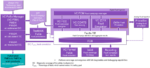
An Example of a Unified Functional Safety Verification Solution
Modern functional safety verification demands far more than isolated fault simulation runs or disconnected analysis tools. As semiconductor designs grow in complexity, the verification challenge increasingly requires a unified methodology capable of connecting architectural safety intent, FMEDA data, RTL implementation, software workloads, and safety metrics into a single coherent flow.
From an EDA technology perspective several key technologies are needed: Fast fault simulation and emulation, formal fault reduction, fault probability calculation, fault campaign management, fault coverage and debug and all of that connecting to a unified fault database. Figure 1 shows an example.
Table I shows typical results a user should expect on a RISC-V reference design and a SoC design.
| RISC-V Design | VC Z01X | ZeBu | |
| Wall Clock | Compile | 34sec | 1hr 50min |
| Runtime (Linux Boot) | > 4 months (estimated) | 7hr 22 min | |
| SoC Design | VC Z01X | ZeBu | |
| Wall clock | Compile | 35sec | 7hr 8min |
| Runtime (Linux Boot) | 39hr 25min | 4hr 52min@1Host
58min@8Hosts |
|
| Fault Results | Number of Hard Faults | 133 (Hyper Faults) Dropped from Fault Simulation | Detected: 101
Not-detected: 32 |
| Runtime | > 40hr 20min | 12hr@1Host | |
Table I: Benchmark results highlighting the throughput and accuracy-of-results (Source: Synopsys)
In both test cases, the data illustrates how fault emulation complements traditional fault simulation by enabling the execution of dramatically longer software workloads while simultaneously achieving levels of fault coverage closure that would be impossible to reach through simulation alone. The benchmarks also underscore the remarkable gains obtained not only in raw performance, but also in accuracy-of-results and confidence in the final safety metrics.
Conclusion
Seen in this light, the relationship between classical fault simulation and functional safety verification is not one of replacement, but of transformation. The foundational ideas developed in the context of traditional fault simulation, that is, modeling faults, propagating their effects, and measuring coverage, remain relevant. However, the scope of verification has expanded dramatically. Today’s safety-critical systems must be validated not only at the hardware level, but also in the context of software behavior, safety mechanisms, system interactions, and real-world operating conditions.
This shift has elevated fault emulation from performance optimization to a critical enabler of functional safety verification. By executing large-scale fault campaigns at near-realistic speeds, fault emulation makes it practical to evaluate millions of fault scenarios across complex hardware-software systems and generate the coverage data required for FMEDA analysis.
Yet fault emulation alone is not enough. The value lies not merely in the speed of the underlying hardware engines, but in their integration into a broader software-defined safety verification flow. Automated fault classification, safety metric calculation, campaign management, results analysis, and traceability are all essential components of a complete FMEDA methodology. Together, these capabilities bridge the gap between low-level fault behavior and system-level safety goals, enabling development teams to achieve the rigorous diagnostic coverage demanded by modern standards such as ISO 26262.
As systems continue to grow in complexity, this combination of fault emulation and software-driven safety analysis will remain a cornerstone of functional safety verification.
Also Read:
All-Embracing Multiphysics Analysis for Chiplet-Based Systems
Podcast EP351: A Detailed Overview of the Emerging Standards for 400G with Kent Lusted