

Semiconductor manufacturing has become one of the most data-intensive industrial environments in the world, and AI is rapidly becoming central to how fabs operate and optimize. Yet, rather than converging on a single model for AI adoption, the industry is evolving along two distinct paths. One centered on platform-scale integration and the other on fast, point-level deployment. The two approaches reflect differences in market structure, customer expectations, vendor ecosystems, and cultural approaches to manufacturing. This article explores these two models not as competing answers, but as context-driven responses to different operating environments, with the long-term outcome still open.
Global Semiconductor AI Context
The increasing complexity of semiconductor devices and manufacturing processes has led to an explosion in data generation, often reaching millions of parameters per device and petabyte-scale datasets per fab. At the same time, the industry must accelerate new product introduction while maintaining yield and stability in mass production. These pressures have made AI a necessary layer in semiconductor manufacturing, enabling scalable analysis, automation of decision-making, and interpretation of complex process interactions.
Modern AI systems in this space are typically built on a combination of scalable analytics engines, structured workflows, and domain-specific knowledge, often enhanced by natural language interfaces. While these foundational elements are broadly consistent across regions, how they are packaged, deployed, and monetized varies significantly.
Reference Architecture (Platform AI as a Model)
One way to understand these differences is through a reference architecture that represents a platform-based approach to semiconductor manufacturing AI.
At its core is a scalable analytics engine designed to process extremely large and complex datasets using parallel computation. This enables real-time or near-real-time analysis across vast manufacturing data environments.
Above this sits a workflow layer that defines how analytics are structured and executed. In this model, workflows act as a system-level language, capturing logic, enabling reuse, and providing traceability. They also function as a form of long-term system memory, embedding best practices and analytical patterns.
A natural language interface layer allows engineers to interact with the system more intuitively, translating human intent into structured workflows. This improves accessibility but relies on the underlying system for execution.
Finally, a semiconductor domain knowledge layer provides the contextual intelligence needed to interpret data correctly. This layer encodes device physics, process interactions, and historical expertise, ensuring that AI outputs are grounded in real manufacturing behavior rather than purely statistical patterns.
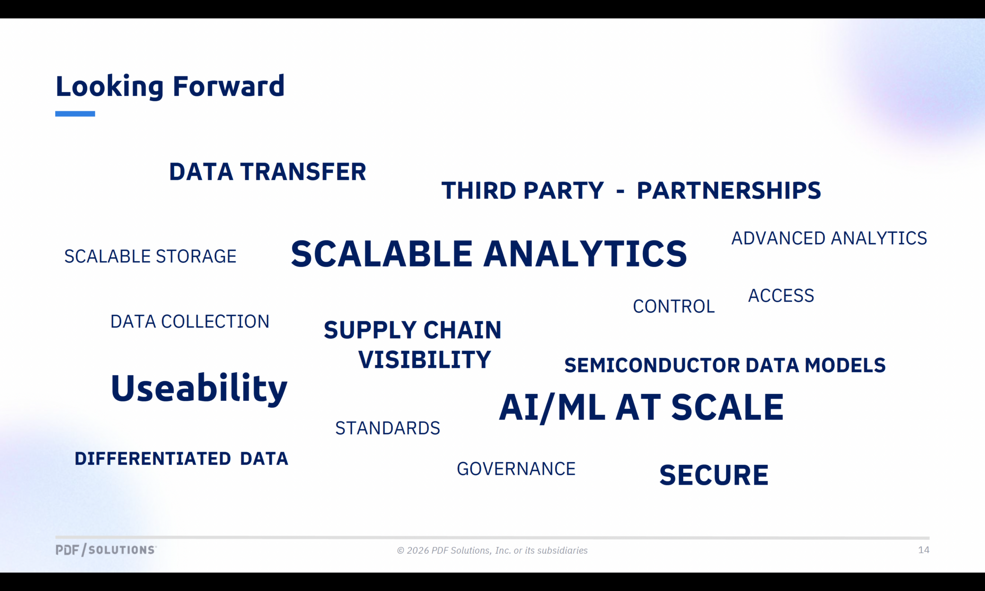
This architecture reflects a platform-oriented philosophy, where AI is treated as infrastructure rather than a collection of isolated tools. At its latest Users Conference PDF Solutions introduced the overall architecture of its platform and AI strategy, and demonstrated how LLMs integrated with this platform can be used to answer complex semiconductor manufacturing analytics questions using natural language.
Core Market Divergence: Platform vs. Point Solutions
In North America and Europe, semiconductor AI has largely evolved around platform-based deployment models. AI systems are designed as foundational layers that integrate with existing manufacturing systems and support multiple use cases over time. This approach emphasizes consistency, scalability, and long-term value creation. Because these environments often involve complex legacy systems, platforms serve as a unifying layer that can bridge data and processes across the fab. Deployment tends to be methodical, with significant emphasis on validation and integration.
In China, a different pattern has emerged. AI adoption is often driven by forward-deployed, point-specific solutions that address immediate manufacturing challenges. Many vendors are smaller and highly specialized and work closely with fabs and equipment providers to develop targeted applications for specific problems such as tool matching, chamber variation, or yield excursions. These solutions are deployed quickly, refined through direct feedback, and expanded incrementally to other problem areas. Rather than building a unified platform upfront, the system evolves through a series of practical implementations.
Structural Drivers Behind the Divergence
These two approaches are shaped by a combination of structural and cultural factors. In China, the prevalence of smaller AI vendors creates a strong need for rapid monetization, which favors solutions that can be developed and deployed quickly with clear, measurable outcomes. The manufacturing environment also places a high value on immediate operational improvements, reinforcing a preference for short deployment cycles and tangible results.
In North America and Europe, semiconductor companies often operate within more mature ecosystems that include extensive legacy infrastructure. This creates a need for integration and consistency across systems, making platform-based approaches more attractive. There is also a greater tolerance for longer deployment timelines when the expected outcome is system-wide optimization and long-term efficiency gains.
These differences do not reflect a gap in capability, but rather different priorities shaped by market conditions and organizational context.
Trade-offs Between the Two Approaches
Each model offers distinct advantages and challenges. Platform-based approaches provide a structured foundation that can support multiple use cases, enable cross-system optimization, and reduce redundancy over time. They are particularly well-suited for large-scale environments where integration and consistency are critical. However, they can require significant upfront investment and may take longer to deliver visible results.
Point-solution approaches, by contrast, are highly effective at delivering rapid impact. By focusing on specific problems, they can be deployed quickly and aligned closely with operational needs. This makes them well-suited for environments where speed and measurable outcomes are prioritized. At the same time, the accumulation of independent solutions can introduce fragmentation, making it more difficult to achieve system-wide optimization or maintain consistency across processes.
Importantly, these trade-offs are not absolute; they reflect different ways of balancing speed, scale, and integration.
Strategic Hybrid Possibility
Rather than converging entirely toward one model, there is growing recognition that elements of both approaches may coexist. A platform layer can provide structure, scalability, and domain intelligence, while localized solutions can continue to address specific operational challenges quickly and effectively. In such a model, platforms may evolve to incorporate or orchestrate point solutions, creating a layered system that combines integration with flexibility.
Whether and how this hybrid model develops will depend on how vendors and customers navigate the balance between standardization and customization, as well as how ecosystems mature over time.
Summary
The current landscape of semiconductor manufacturing AI reflects not a single direction of travel, but a divergence shaped by real-world constraints and priorities. Platform-centric and point-solution approaches each represent viable responses to different environments, and both are likely to continue evolving. Over time, one model may prove more scalable or sustainable, or a hybrid approach may emerge as dominant. For now, understanding the underlying drivers of each model is more important than determining a definitive long term winner.
Learn more at PDF Solutions.
Also Read:
WEBINAR: Beyond Moore’s Law and The Future of Semiconductor Manufacturing Intelligence
Operationalizing Secure Semiconductor Collaboration: Safely, Globally, and at Scale
Why PDF Solutions Is Positioning Itself at the Center of the Semiconductor Ecosystem
Share this post via:


Comments
There are no comments yet.
You must register or log in to view/post comments.