Although the high-performance X-NAND memory cell and architecture were first introduced in 2020 by Neo Semiconductor, designers at Neo haven’t rested on that accomplishment and recently updated the cell and the architecture in a second-generation implementation to achieve 20X the performance of conventional quad-level-cell (QLC) 3D NAND memories. The Gen2 X-NAND, unveiled at this month’s Flash Memory Summit, achieves that improvement through an enhanced architecture that allows the 3D NAND flash programming (i.e., data writes) to occur in parallel using fewer planes. Able to deliver a 2X performance improvement over the first generation X-NAND technology, the Gen2 architecture remains compatible with current manufacturing technologies and processes thus giving adopters of the technology a competitive advantage over existing 3D NAND flash memory products.
According to Andy Hsu, Neo’s CEO, the Gen2 technology incorporates zero-impact architectural and design changes that do not increase manufacturing costs while offering improvements in throughput and reductions in latency. The X-NAND technology can be implemented with all flash cell structures – SLC, MLC, TLC, QLC, and PLC – while delivering higher performance at comparable manufacturing costs. Neo is currently looking to partner with memory manufacturers who will license the X-NAND technology and then design and manufacture the high-performance memory chips.
NAND-flash memories based on the QLC cell and 3D stacking have been widely adopted in many applications thanks to the high storage capacities possible and their relatively low cost per bit. The one drawback is their slow write speed. The X-NAND technology overcomes that limitation and improves the QLC NAND read and write speeds threefold and the sequential read/write throughput by 15 to 30X. Further improvements in the Gen2 technology let memories deliver SLC-like (single-level cell) performance but with the higher capacity and lower cost of QLC implementations. Transfer rates of up to 3.2 Gbytes/s are possible with the Gen2 X-NAND technology.
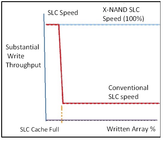
In Neo’s Gen1 design the company employs a unique SLC/QLC parallel programming scheme that allows the data to be programmed to QLC pages at SLC speed for the entire memory capacity. This also solves the conventional NAND’s SLC cache-full problem (see the figure). When the conventional SLC cache is full for traditional NAND, the data will be directly written to QLC cells, and the write speed will be reduced to below 12%. X-NAND solves this problem, explains Hsu, and it also provides an excellent solution for heavy-write systems such as data centers with NAS systems.
Furthermore, the X-NAND’s 16-64 plane architecture provides parallelism at the chip level. When compared to a conventional NAND that uses 2 to 4 planes, one X-NAND chip can provide the same parallelism of 4 to 16 NAND chips. This would allow small-form-factor packaging such as in M.2 and eMMC memory modules. Additionally, X-NAND’s bit-line capacitance is only 1/4 – 1/16 that of a conventional NAND and thus the bit line’s power consumption for read and write operations can be reduced to about 1/4 – 1/16 (or by about 25% – 90%). This significantly increases the battery life for smartphones, tablets, and IoT devices.
Also read:
WEBINAR: A Revolution in Prototyping and Emulation
ARC Processor Summit 2022 Your embedded edge starts here!
WEBINAR: Design and Verify State-of-the-Art RFICs using Synopsys / Ansys Custom Design Flow
Share this post via:


Is Intel About to Take Flight?