I was asked to give a talk at the 2021 ISS conference and the following is a write up of the talk.
The title of the talk is “Logic Leadership in the PPAC era”.
The talk is broken up into three main sections:
- Background information explaining PPAC and Standard Cells.
- A node-by-node comparisons of companies running leading edge logic processes.
- PPAC trend charts by company and year.
Background Information
Historically new processes have targeted Power, Performance and Area (PPA), for example during TSMC’s 2020-Q1 conference call they stated that their 3nm process would provide 25-30% lower power at the same speed relative to 5nm, 10-15% better speed at the same power and a 70% increase in density.
With rising costs and challenges to produce cost effective leading edge processes the need to target cost during process development has become apparent. For example, both Imec and Applied Materials have discussed PPAC in recent presentations.
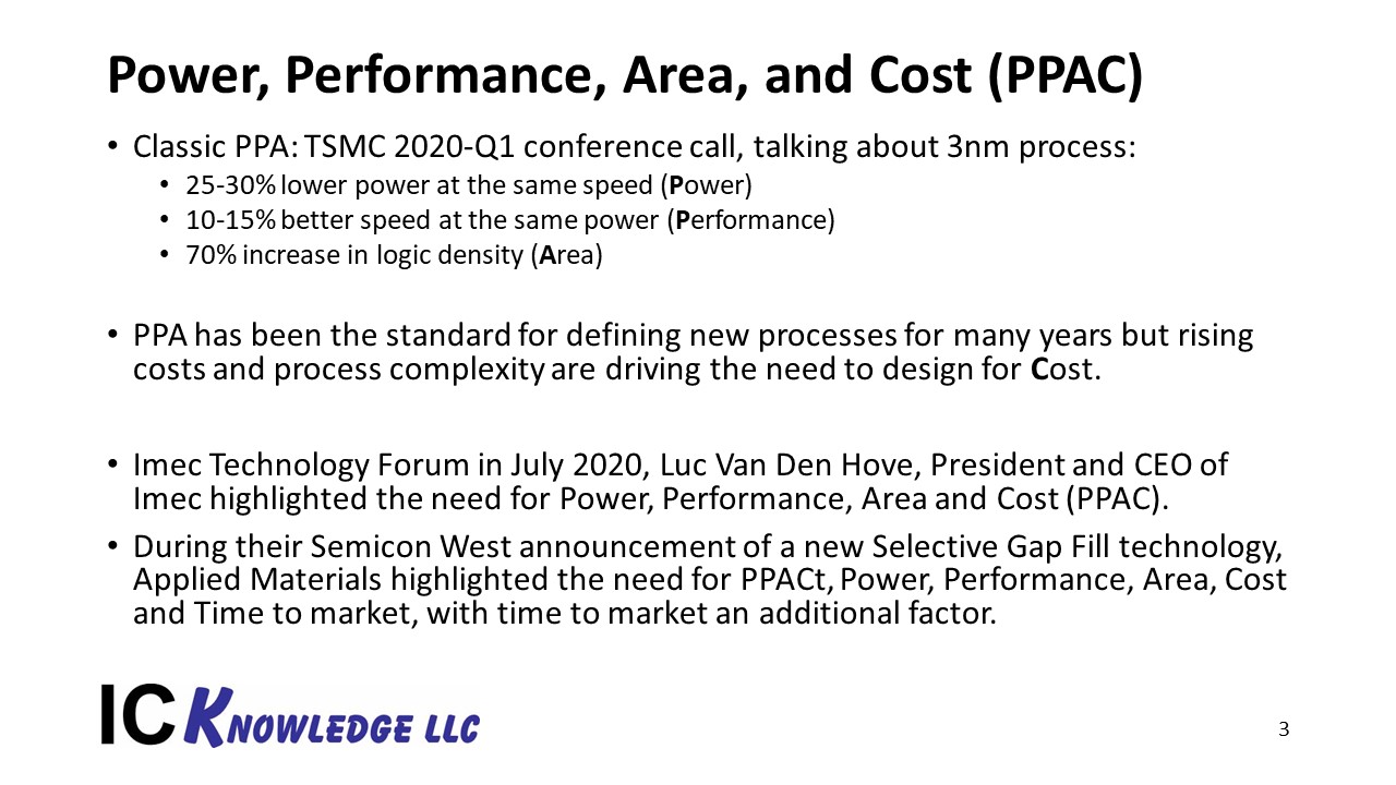
Figure 1. Power, Performance, Area and Cost (PPAC).
Logic designs are created using standard cells, inverters, NAND gates, Scanned Flip Flops, etc.
The size of a standard cell is determined by the cell type and the design rules of the process the cell is run on. Process minimum dimensions can be used to calculate cell sizes. The height of a standard cell is determined by the minimum metal pitch multiplied by the number of tracks. The cell width is some number of contacted poly pitches plus an extra contacted poly pitch is required at the edge of the cell for a double diffusion break cell.
In recent years difficulties shrinking pitches has led to track reductions to scale down cell sizes, however as track heights are reduced it leads to fin depopulation, for a 9-track cell each transistor can have 4 fins, for a 7.5-track cell only 3 fins fit for each transistor and for 6-track cells that are the current state-of-the-art, only 2 fins fit in the cell per transistor. All other things being equal a 6-track cell with 2 fins per transistor will have one-half the drive current of a 9-track cell with 4 fins per transistor. This has led to Design-Technology-Co-Optimization (DTCO) where a new process is developed to support a 6-track cell with 2 fins per transistor, the fins are designed to provide higher drive current per fin for example by making them taller.
When comparing process density, we use the smallest cell available on each process (least tracks) to calculate millions of transistors per millimeter squared. We assume a design with 60% NAND cell and 20% Scanned Flip Flops.
A lot of people try to compare processes based on transistor density for an actual design, the problem with this is processes support multiple cell heights, for example 6 and 9-track cells, A design that targets high performance would use a lot of 9-track cells and a process that targets lower performance but minimum size would use a lot of 6-track cells, even on the same process two different designs targeting different performance levels would have different densities, we therefore use the minimum available cells to do a fair comparison.
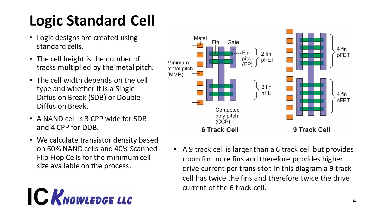
Figure 2. Standard Cell.
Another key density comparison for logic processes is SRAM cell size since many designs incorporate significant amounts of SRAM cache.
A have written an article on design effects on process density that is available here.
Node by Node Comparison
The node-by-node comparison begins with 28nm foundry processes versus intel’s 22nm process. This comparison represents a moment in time as opposed to the same nodes where foundry 20nm nodes might be more appropriate.
In 2011 Intel introduced their 22nm process with the world’s first FinFET production, at the same time the foundries were producing 28nm planar devices. From a device technology perspective 28nm represented the foundries introduction of High-K Metal Gate (HKMG), a technology Intel introduced in 2007 and now Intel is introducing FinFETs and the foundries will not introduce FinFETs for three more years. At this point in time Intel was the clear logic technology process leader.
Interestingly, the Intel 22nm process has the best SRAM cell size but for logic has lower transistor density than the foundry 28nm processes, although presumably better performance. Intel was conservative on some process dimensions presumably because this was their first FinFET generation.
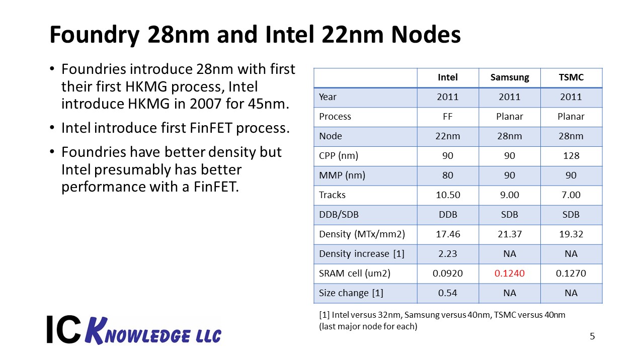
Figure 3. Foundry 28nm and Intel 22nm Nodes.
Moving forward to 2014 Intel introduces their second generation FinFET process with an aggressive shrink that put them into the lead on both logic density and SRAM cell size. In 2014 Samsung introduced their first generation FinFET with their 14nm process and in 2015 TSMC introduced their first generation FinFET with their 16nm process.
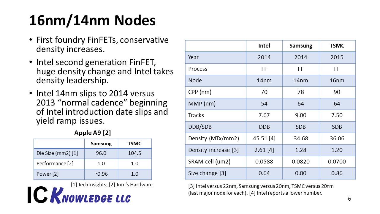
Figure 4. 16nm/14nm Nodes.
A key point at this node is that Intel 14nm was originally due in 2013 and even when it was introduced suffered from a slow yield ramp, this was the beginning of a chain of intel delays and yield problems that persist today.
Another thing that stands out at this node is that Apple designed their A9 processor based on Samsung’s 14nm process but then also ported the design to TSMC’s 16nm process. Tom’s Hardware compared the PPA for the A9 on both processes and found power to be slightly better on the Samsung process, performance the same for both and die area to also be slightly smaller on the Samsung process. The Samsung power and area advantage may just be because the part was originally designed for Samsung and later ported to TSMC, but it gives us a unique opportunity to compare the two processes. We will use this data point later as a starting point for some of the trend analysis we will present.
The next step in time is the instruction of foundry 10nm nodes in 2016 when both Samsung and TSMC took the process density lead from Intel. This is the beginning of a key difference between Intel and the foundries where Intel takes bigger density jumps with each successive process generation, but the foundries introduce new generations faster and pass Intel for process leadership.
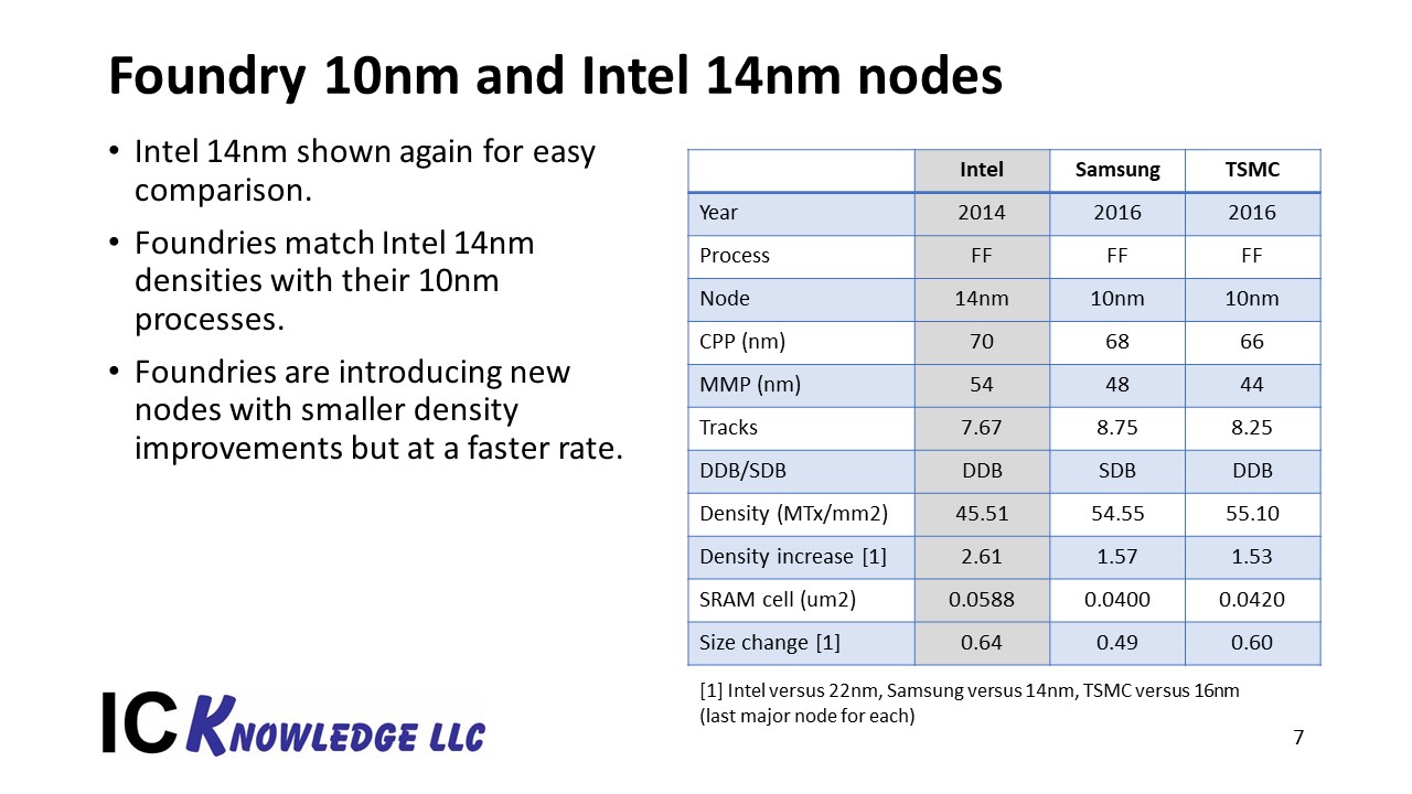
Figure 5. Foundry 10nm and intel 14nm nodes.
Stepping forward again, TSMC introduces their 7nm process in 2017, Samsung introduced their 7nm process in 2018 and Intel’s 10nm process finally enters production in 2019, although even today Intel is struggling with yield on 10nm. Intel’s 10nm process did move them into relative logic density parity with the foundry 7nm processes but with larger SRAM cell sizes. It should also be noted that as we will see in a moment, in 2019 the foundries began production on 5nm processes that once again moved them ahead.
At 7nm Samsung’s process has several EUV layers and for their internal production was the first production EUV process, although TSMCs 7nm+ process that added EUV for several layers may have been the first generally available foundry process with EUV. Total EUV layers for 7nm was between 5 and 7.
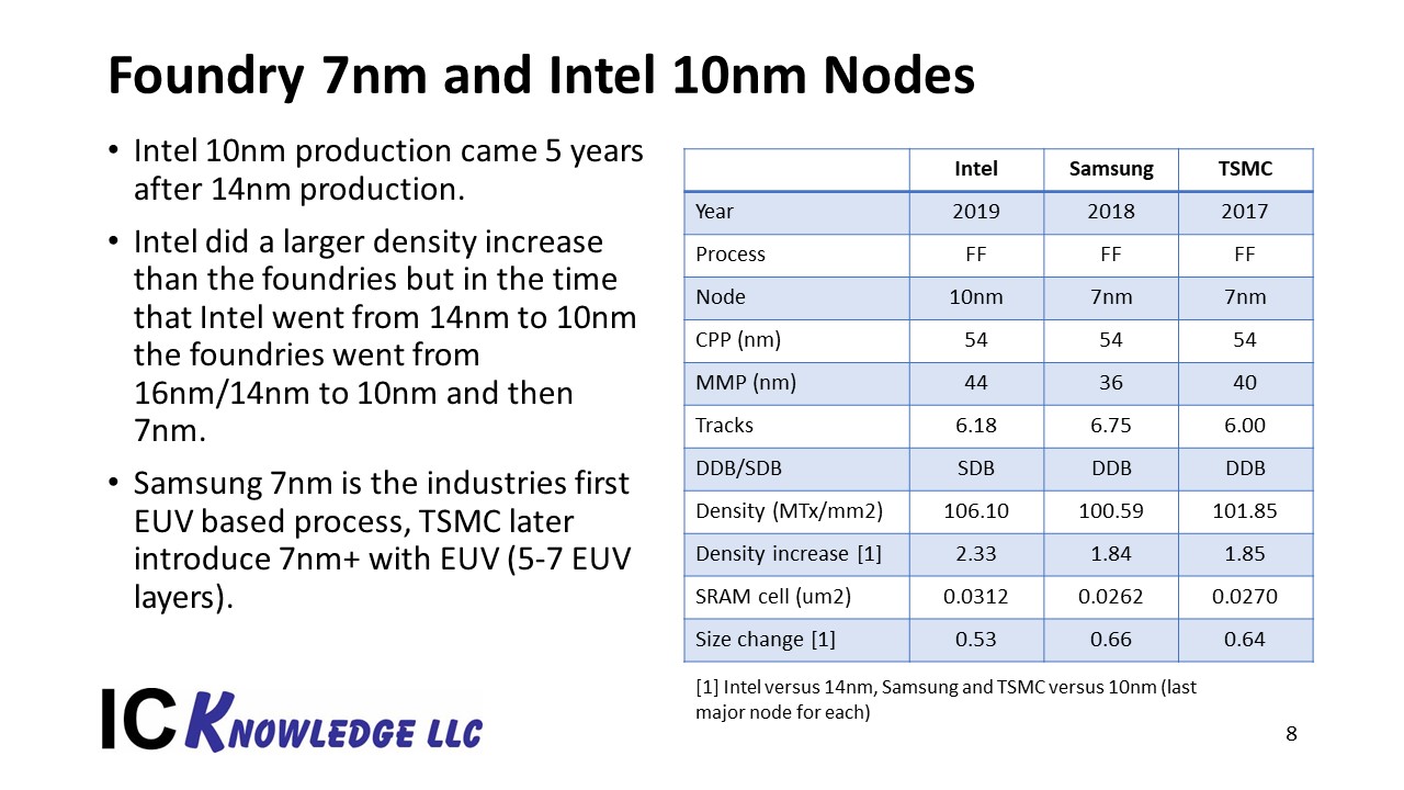
Figure 6. Foundry 7nm and Intel 10nm Nodes.
In late 2019 we saw the foundries begin risk starts of 5nm processes and those processes reached high volume production in 2020. At the Intel 10nm/Foundry 7nm node the three companies had similar logic densities. Moving to 5nm TSMC delivered an approximately 1.8x density improvement while Samsung only delivered a 1.33x density improvement, this leads to TSMC having a substantial logic density advantage and the smallest SRAM cell size. 5nm also saw an increase in EUV layers to 10 to 15 layers and TSMC introduced a pFET with a high mobility Silicon-Germanium fin. While the foundries are once again delivering a new node, Intel is still working on ramping up 10nm yields.
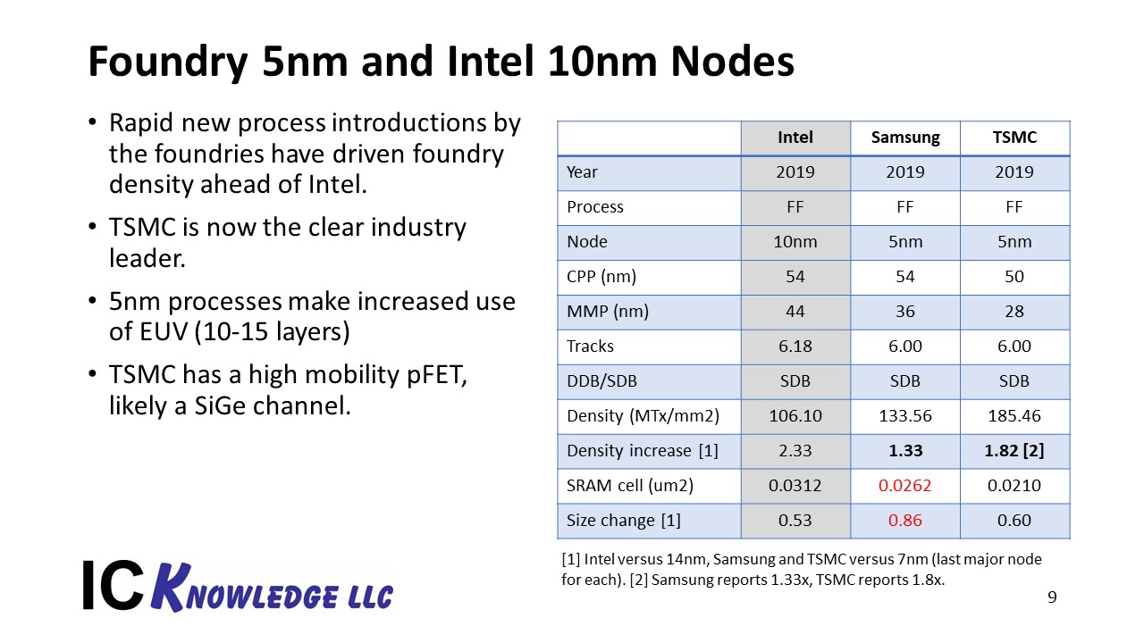
Figure 7. Foundry 5nm and Intel 10nm Nodes.
Now we step forward into the future with foundry 3nm processes starting risk starts in 2021 with 2022 production, and Intel 7nm process entering production in 2022. Intel’s 7nm was originally due in 2021 so 2022 represents another delay and there are rumors it will be delayed beyond 2022. There have also been reports of delays for Samsung and TSMC 3nm, our check indicate Samsung may be delayed but TSMC is on track.
Intel 7nm will represent Intel’s first use of EUV and Samsung’s 3nm will see the industry’s first use of Gate-All-Around (GAA) in the form of stacked Horizontal-Nano-Sheets (HNS). TSMC is continuing to utilize FinFETs at 3nm.
For 7nm Intel has announced a 2x density increase over 10nm, Samsung has announced 3nm will be 1.35x denser than 5nm and TSMC has announced 3nm will be 1.7x denser than 5nm. Based on these announced density improvements TSMC will have the densest process by a wide margin, Intel will pass Samsung for second place and Samsung will be in third. We expect 15 to 30 EUV layers at this node with TSMC at the upper end due to their denser process.
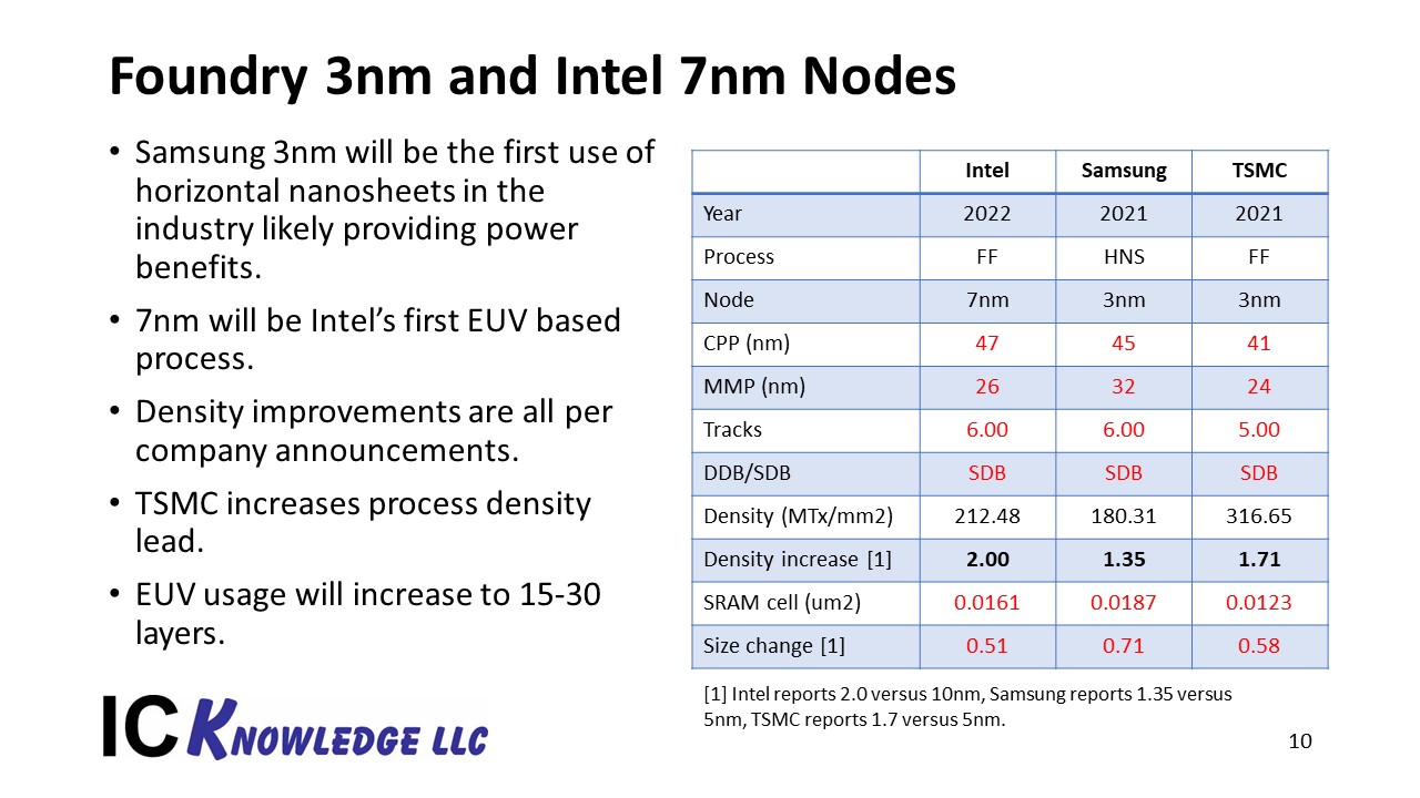
Figure 8. Foundry 3nm and Intel 7nm Nodes.
There has been a lot of speculation about whether Intel will outsource production of their microprocessors to the foundries given that the foundries now have the process lead. At the Credit Suisse conference in December 2020, Intel CEO Robert Swan announced Intel will continue to develop leading edge process with Intel 5nm and 3nm processes still planned. I wouldn’t be surprised to see Intel gradually outsource more of their needs, but it doesn’t currently look like any radical change is going to take place any time soon. I should also point out that given Intel’s volumes it would take years for the foundries years to ramp up to accommodate Intel’s volumes.
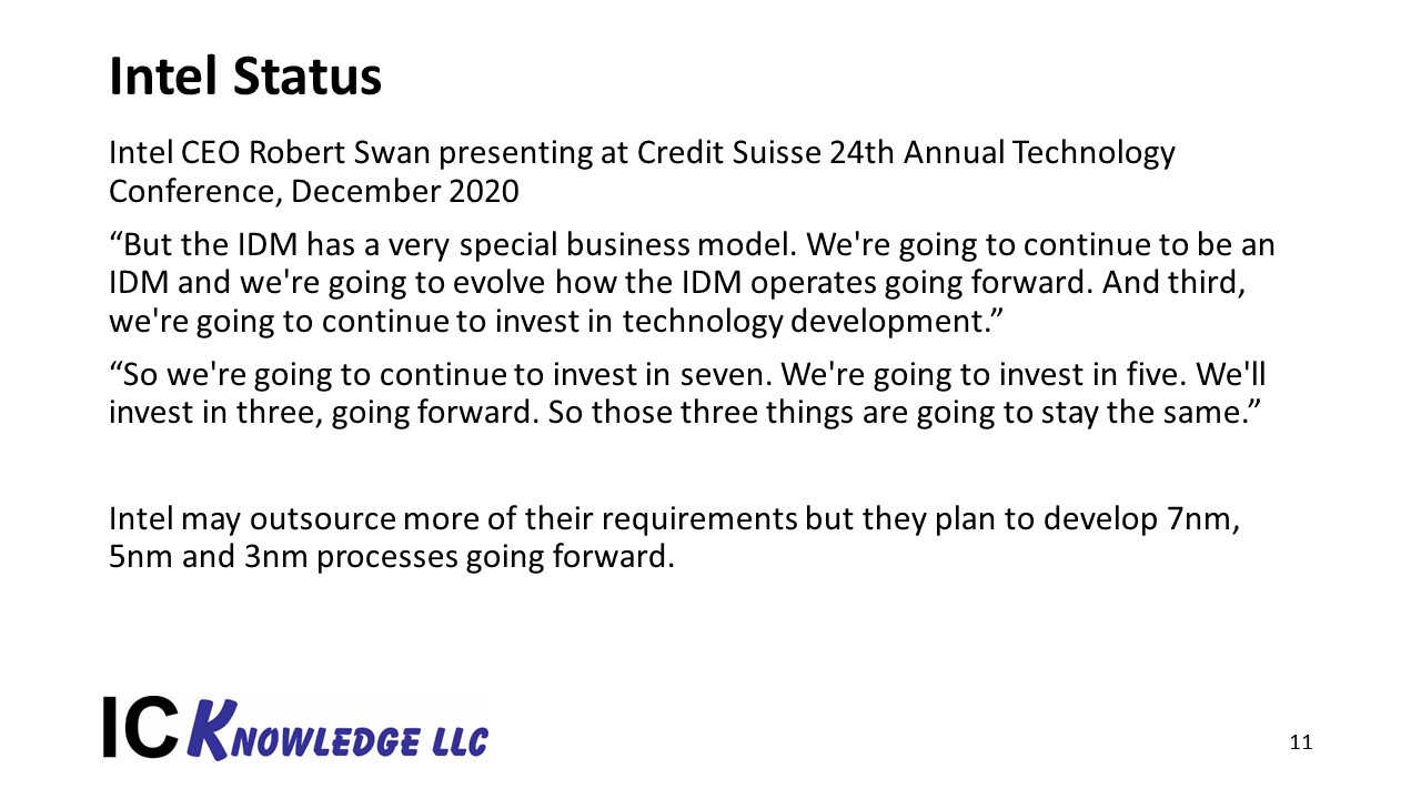
Figure 9. Intel Status
PPAC Trends
Now we will compare PPAC by company and time.
One key take-away from our analysis is that although Intel tends to make bigger logic density improvements from each new node the foundries are introducing new nodes faster and ultimately driving density faster. In fact, between 2014 and 2022 the foundries will have introduced five new nodes in the time it took Intel to introduce three new nodes and this is only counting major nodes, the foundries have introduced a lot of half-nodes as well. Intel does introduce “half-nodes” as well with +, +++, +++ nodes but they are performance half-nodes, not shrinks.
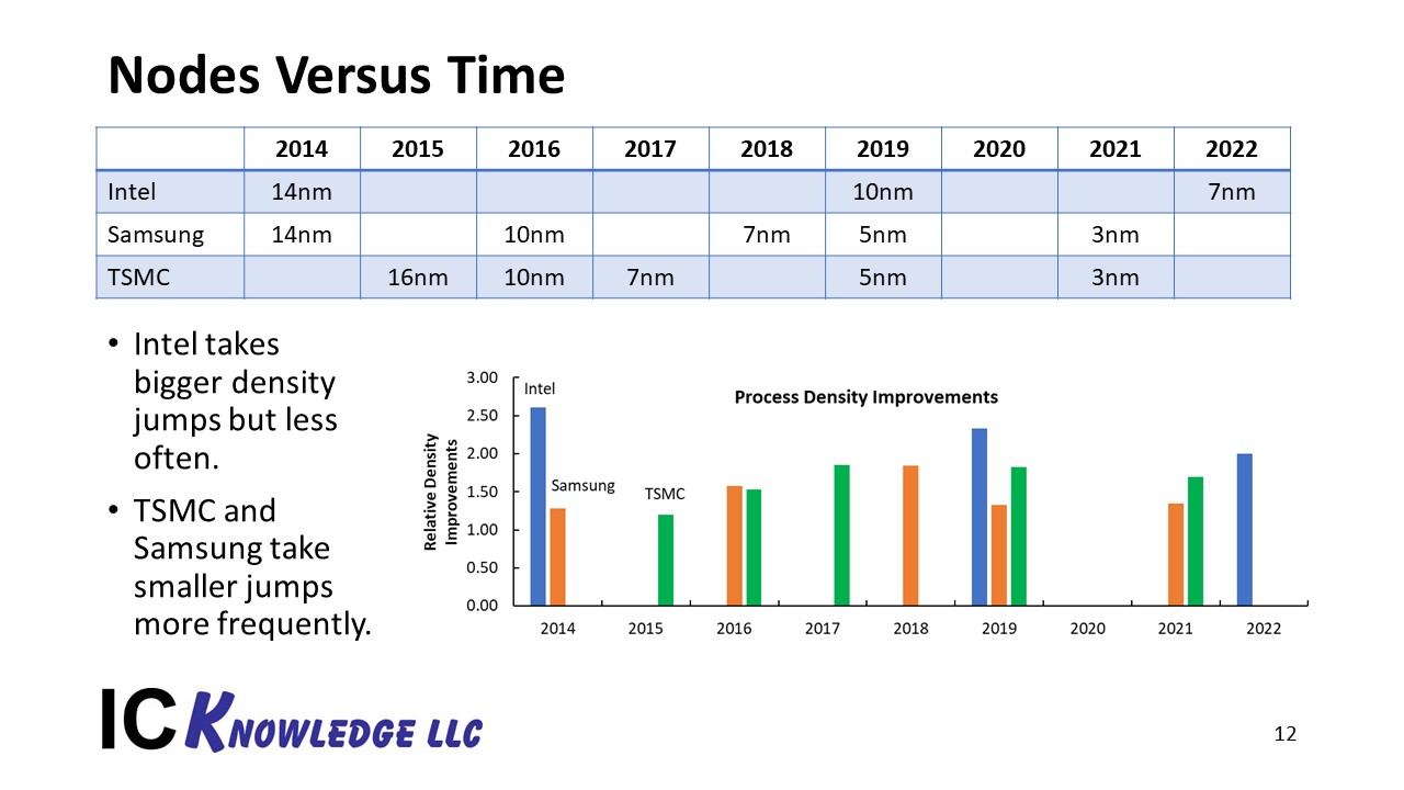
Figure 10. Nodes Versus Times.
Comparing Power and Performance between companies and process is nearly impossible, ideally someone would run a consistent product such as an Arm core with a set amount of SRAM cache on each process and publish power and performance metrics, but this is way too expensive to be practical. In the chart in figure 10. I have created the best estimated comparison I can produce.
I stared the power comparisons at the 16nm/14nm node where we have the A9 on both Samsung 14nm and TSMC 16nm. I have given Samsung a slight advantage as previously discussed even though this may be a design issue. I have then taken the power improvement for each subsequent node from the companies announced improvements. As can be seen TSMC takes a significant lead at 10nm, Samsung does largely catch up a 3nm presumably reflecting their switch to HNS although TSMC is still competitive with their high scaled FinFET. I am unable to place Intel on this chart with any confidence.
For the performance comparison I once again start with the A9 at the Samsung 14nm and TSMC 16nm node and use the companies announced performance improvement by node to forward project. TSMC’s develops a performance advantage over Samsung at 10nm and increases their lead at each successive node. To place Intel on this chart I looked at the Intel microprocessors made on their 10nm Super Fin process and AMD microprocessors made on TSMC’s 7nm process and concluded they have similar performance. I also used published Intel performance comparisons between their base 14nm process and 10nm Super Fin process to back project how Intel would compare at the 14nm/16nm node. TSMC and Intel are competitive at the Intel 10nm/Foundry 7nm node with Samsung likely having the lowest performance. I don’t have 7nm performance estimates from Intel, but my “best guess” would be TSMC 3nm will be as good or better.
I do want to stress that these are “best estimates” with a lot of uncertainty.
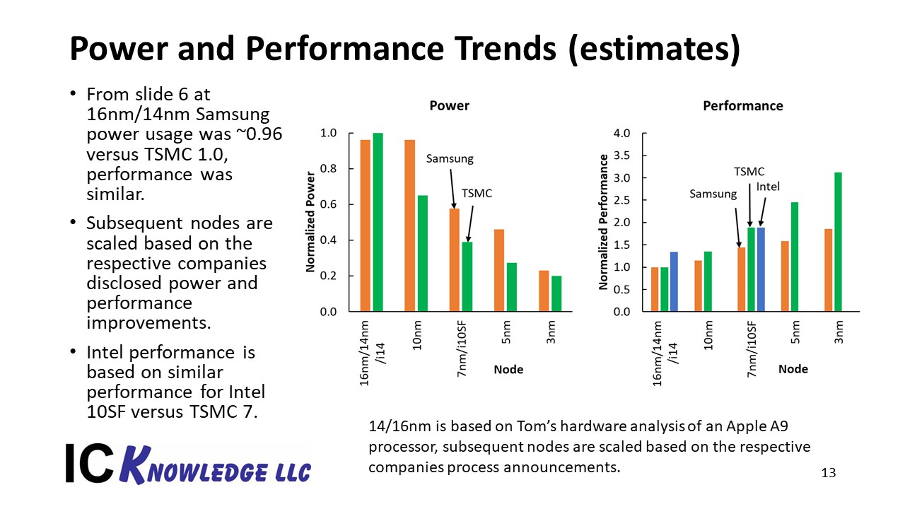
Figure 11. Power and Performance Trends.
This finally bring us to Cost.
My company IC Knowledge LLC is the world leader in cost and price modeling of semiconductors and MEMS. Our commercially available Strategic Cost and Price Model is a company specific industry roadmap beginning with the first 300mm processes and projecting out into the late 2020’s for 3DNAND, 3DXPoint, DRAM and Logic. The Strategic Cost and Price Model produces equipment, materials and manufacturing cost and selling price estimates by company, time, and even specific wafer fabs. Using the Strategic Cost and Price Model I have produced the three trend plots on the next slide.
On the left is the normalized wafer cost by node. Some key points on this chart:
- The wafer costs do not include mask set amortization. For foundries masks are typically purchased by the customer and not part of the wafer price when the wafers are sold to the customer. For Intel mask amortization costs would typically be included but to make the comparisons consistent company to company we have omitted mask amortization. There is an important point that mask costs are increasing rapidly and wafer costs with mask set amortization are highly sensitive to the volume the masks are amortized over. Rising mask costs have resulted in a situation where leading-edge processes only make sense for high volume designs.
- The wafers cost also don’t consider design costs, this is another area where costs are rapidly increasing and pricing out all but the largest volume products from leading edge processes.
- For this analysis we have assumed new greenfield fabs for each node with Intel fabs located in the united states, Samsung in South Korea and TSMC in Taiwan.
The resulting wafer cost plot shows rising wafer costs with Intel having the highest wafer costs until the Intel 7nm/Foundry 3nm node where TSMC has the highest costs. This reflects TSMC having the densest process and Intel having fewer interconnect layers.
The middle graph provides normalized logic transistor density based on the values presented in the node-by-node analysis section of our presentation. As previously noted, we expect TSMC to have the densest process at the i7/F3 node.
Finally, the graph on the right side combines wafer cost and transistor density to produce a relative logic transistor cost trend. What is clear in this chart is that although higher transistor density may require a more expensive wafer process, the transistor density improvements, at least in the cases studied overcomes the higher wafer cost to deliver lower transistor cost.
Another key take-away is that for logic transistors Moore’s law is alive and well. In his seminal 1965 Electronics Magazine article “Cramming more components onto integrated circuits”, Gordan Moore stated what became known as Moore’s law: “The complexity for minimum component costs has increased at a rate of roughly a factor of two per year”. The key to me in this “law” is that is as much an economic observation as it is a technology observation. In my opinion the purest measure of Moore’s law is are we continuing to decrease cost per transistor, and as this plot shows, we are, although once again this is purely logic transistor manufacturing cost and these economics only work for high volume products.
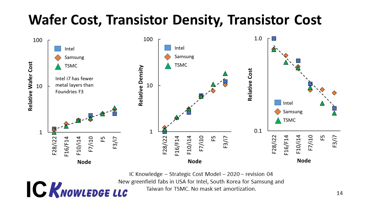
Figure 12. Wafer Cost, Transistor Density, Transistor Cost.
Conclusion
The key points in this presentation around PPAC and logic leadership are summarized in Figure 12.
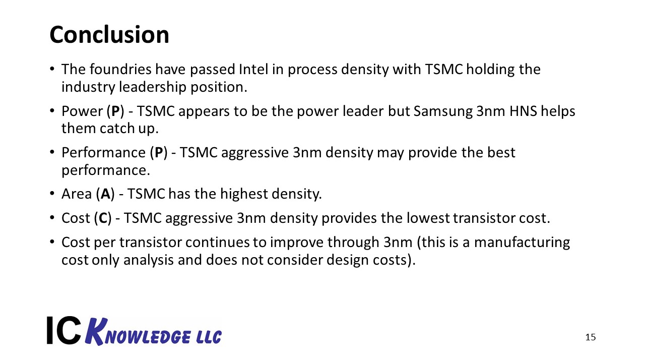
Figure 13. Conclusion.
TSMC’s continued rapid execution of moderate shrinks has led them to a leadership position and we expect them to maintain leadership through the 3nm node and beyond.
Also Read:
No Intel and Samsung are not passing TSMC
Leading Edge Foundry Wafer Prices
Share this post via:


Comments
19 Replies to “ISS 2021 – Scotten W. Jones – Logic Leadership in the PPAC era”
You must register or log in to view/post comments.