
It was an honor to see DR. Chenming Huspeak and to learn more about FinFets, a technology he has championed since 1999. Chenming is considered an expert on the subject and is currently a TSMC Distinguished Professor of Microelectronics at University of California, Berkeley. Prior to that he was the Chief Technology Officer of TSMC. Hu coined the term FinFET 10+ years ago when he and his team built the first CMOS FinFETs and described them in a 1999 IEDM paper. The name FinFET because the transistors (technically known as Field Effect Transistors) look like fins. The fins are the 3D part in the name 3D transistors. Dr. Hu didn’t register patents on the design or manufacturing process to make it as widely available as possible and was confident the industry would adopt it, and he was right.
There is a six part series on YouTube entitled: FinFET-What it is and does for IC products, history and future scaling presented by Chenming, unfortunately it is in Mandarin. I have asked Paul McLellan to blog it since he speaks Mandarin but the slides look identical to what was presented at the keynote so it may be worth a look:
For those of you who have no idea what a FinFet is, watch this Tri-Gate for Dummies video by Intel. They call a FinFet a Tri-Gate transistor which they claim to have invented. I expect they are referring to the name rather than the technology itself. 😉
Probably the most comprehensive article on the subject was published last November by IEEE Spectrum “Transistor Wars: Rival architectures face off in a bid to keep Moore’s Law alive”. This is a must read for all of us semiconductor ecosystemites. See, like Intel I can invent words too.
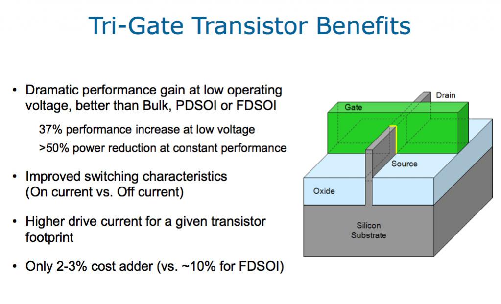
Unfortunately, according to Chenming, lithography will not get easier, double patterning will still be required, and the SoC design and manufacturing cost incremental is still unknown. Intel has stated that there is a +2-3% cost delta but Chenming sidestepped the pricing issue by joking that he is a professor not an economist. In talking to Aart de Geus, Synopsys will be ready for FinFets at 20nm. Since Synopsys has the most complete design flow and semiconductor IP offering they should be the ones to beat in the third dimension, absolutely. You can read about the current Synopsys 3D offerings HERE.

Why the push to FinFets at 20nm you ask? Because of scaling, from 40nm to 28nm we saw significant opportunities for a reduction in die size and power requirements plus an increase in performance. Unfortunately standard planar transistors are not scaling well from 28nm to 20nm, causing a reduction of the power/die savings and performance boost customers have come to expect from a process shrink ( Nvidia Claims TSMC 20nm Will Not Scale?). As a result, TSMC will offer FinFets at the 20nm node, probably as a mid-life node booster, just my opinion of course. Expect 28nm, 20nm, and 14nm roadmap updates at the TSMC 2012 Technology Symposium next week. This is a must attend event! If you are a TSMC customer register HERE.
Why am I excited about transistors in the third dimension? Because it is the single most disruptive technology I will see in my illustrious semiconductor ecosystem career and it makes for good blog fodder. It also challenges the mind and pushes the laws of physics to the limits of our current understanding, that’s why.


Comments
0 Replies to “Synopsys Users Group 2012 Keynote: Dr Chenming Hu and Transistors in the Third Dimension!”
You must register or log in to view/post comments.