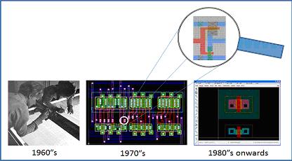
 Have you seen the latest design rule manuals? At 28nm and 20nm design sign-off is no longer just DRC and LVS. These basic components of physical verification are being augmented by an expansive set of yield analysis and critical feature identification capabilities, as well as layout enhancements, printability, and performance validation. Total cycle time is on the rise due to more complex and larger designs, higher error counts, and more verification iterations so we have some work to do here.
Learn how to leverage the superior performance and capacity of the Calibre design-to-silicon (D2S) platform, a comprehensive suite of tools designed to address the complex handoff between design and manufacturing. The Calibre D2S platform offers fast and reliable solutions to design rule checking (DRC), design for manufacturing (DFM), full-chip parasitic extraction (xRC), layout vs. schematic (LVS), silicon vs. layout, and electrical rule checking (ERC).
Target Audience:
IC Design Engineers who are serious about an in-depth evaluation of the Calibre Design-to-Silicon platform.
What you Will Learn:
- Reduce turnaround time with advanced Calibre scaling algorithms and debugging capabilities that directly works within your design environment
- Execute DFM functions and visualize results using Calibre Interactive and RVE
- Understand the benefits of hierarchical vs. flat verification
- Highlight DRC errors in a layout environment by using Calibre RVE
- Learn the concepts of Waivers and hierarchical LVS
- Identify and automatically repair planarity issues in low-density regions
- Identify antennas and understand various repair methods
- Use Calibre’s advanced Nanometer Silicon Modeling capabilities and understand advanced hierarchical parasitic extraction
- Address manufacturability issues by using Calibre DFM tools that help analyze Critical Areas and features
- Understand the importance of identifying LPC hotspots on advanced design nodes
Register Now:
[TABLE]
|-
| Jul 19, 2012
Fremont, CA
| Register
|-
| Aug 16, 2012
Fremont, CA
| Register
|-
| Aug 23, 2012
Irvine, CA
| Register
|-
| Sep 20, 2012
Fremont, CA
| Register
|-
| Oct 18, 2012
Fremont, CA
| Register
|-
| Nov 15, 2012
Fremont, CA
| Register
|-
| Dec 13, 2012
Fremont, CA
| Register
|-
| Jan 17, 2013
Fremont, CA
| Register
|-

How about this, attend the workshop and do a detailed write-up on SemiWiki and I will let you drive my Porsche. This one has the new Porsche Doppelkupplungsgetriebe (PDK) transmission with the Sport Chrono Package. An unforgettable driving experience for sure. Porsche….There is no substitute.


Comments
0 Replies to “Design-to-Silicon Platform Workshops!”
You must register or log in to view/post comments.