This is really the second part to this blog about the challenges of EUV lithography. The next speaker was Franklin Kalk who is CTO of Toppan Photomasks. He too emphasized that we can make almost arbitrarily small features but more and more masks are required (not, that I suspect, he would complain being in the mask business). For EUV to go mainstream the costs must be lower than this and the masks must be defect-free enough. This may happen earlier in memory since the existing built-in redundancy makes it more tolerant of defects.

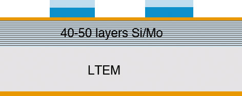
EUV mask blanks consist of a layer of low thermal expansion material, because the mask absorbs about 30% of the EUV light and so gets hot and must not distort. Then 40-50 layers of alternating silicon and molybdenum then a capping layer of ruthenium on top of that (to prevent oxidization). The EUV absorber (where we don’t want the light to reflect) is a tantalum boron nitride film topped with an anti-reflective oxide.
Apart from the obvious fact that this is reflective technology, the other big difference with EUV masks is that mask blanks will never (for the forseeable future anyway) be defect-free. So unlike traditional masks which are essentially blank slates until we pattern them, we need fiducials on the blank so that we can record where the defects are and, subsequently, decide precisely where on the blank to print the pattern to best avoid them. In fact it gets worse. Today we can’t even find all the defects that will print because we are reaching the limits of what we can see even with a scanning-electron-microscope (SEM).
Obviously the fewer defects there are, the better. There has been a lot of progress at reducing pit defects without adding particles and blank yield is improving but there is still a lot of work to do. Sematech’s numbers were that they have defects down to 9 at 50nm and 12 at 40nm. The reticle is typically 4X the wafer so 40nm on the mask translates into 10nm on the wafer.
So how do we avoid defects, given that they will exist? We want all the defects to fall on parts of the mask where we block the EUV light (corresponding to a place on the wafer where we don’t want to expose the photoresist). We can rotate the blank to all four positions. In principle we could shift the pattern on the blank too, but today we cannot yet shift accurately enough off the fiducials on the blank.
Synopsys did some research into this and took 7 designs (I think this actually means mask layers) and 10 actual mask blanks with data on where the defects were. It turns out that every blank could be used in at least 3 of the designs and every design had at least 2 usable blanks.
The full toolkit to be able to find the defects, shift the mask to avoid defects and so on is not expected to be ready until 2018. But Sematech thinks that the first year for high volume manufacturing will be 2015, and they will need 4-5,000 quality blanks with an estimated 45-50% yield to good masks.

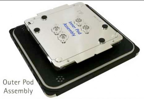
Because EUV masks are used in a vacuum, they need a complicated pod with an outer and inner assembly. The inner assembly goes into the stepper where it is pumped down to a vacuum.
There are also the unknown unknowns that will show up after insertion of EUV into volume manufacturing. With refractive masks we had surprises: haze after 5 years and millions of exposures, for example. With EUV masks there are sure to be similar issues. Masks simply are not indestructible.


Is Intel About to Take Flight?